Method for manufacturing image display device and image display device

A technology of an image display device and a manufacturing method, applied in the directions of instruments, optics, nonlinear optics, etc., can solve the problems of liquid crystal cell gap change, ripple, visibility problems, etc.

Inactive Publication Date: 2020-10-23
NIPPON KAYAKU CO LTD
View PDF18 Cites 0 Cited by
  • Summary
  • Abstract
  • Description
  • Claims
  • Application Information

AI Technical Summary

Problems solved by technology

[0005] However, in the case of producing an image display device by the above-mentioned method, after forming the cured product layer, if the weir portion of the cured ultraviolet curable resin is pressed with a finger or the like, force may be locally applied to the pressed portion, resulting in The gap of the liquid crystal cell changes, which causes ripples, causing problems in visibility when pressing

Method used


Image

  • Method for manufacturing image display device and image display device
  • Method for manufacturing image display device and image display device
  • Method for manufacturing image display device and image display device

Examples


no. 1 approach

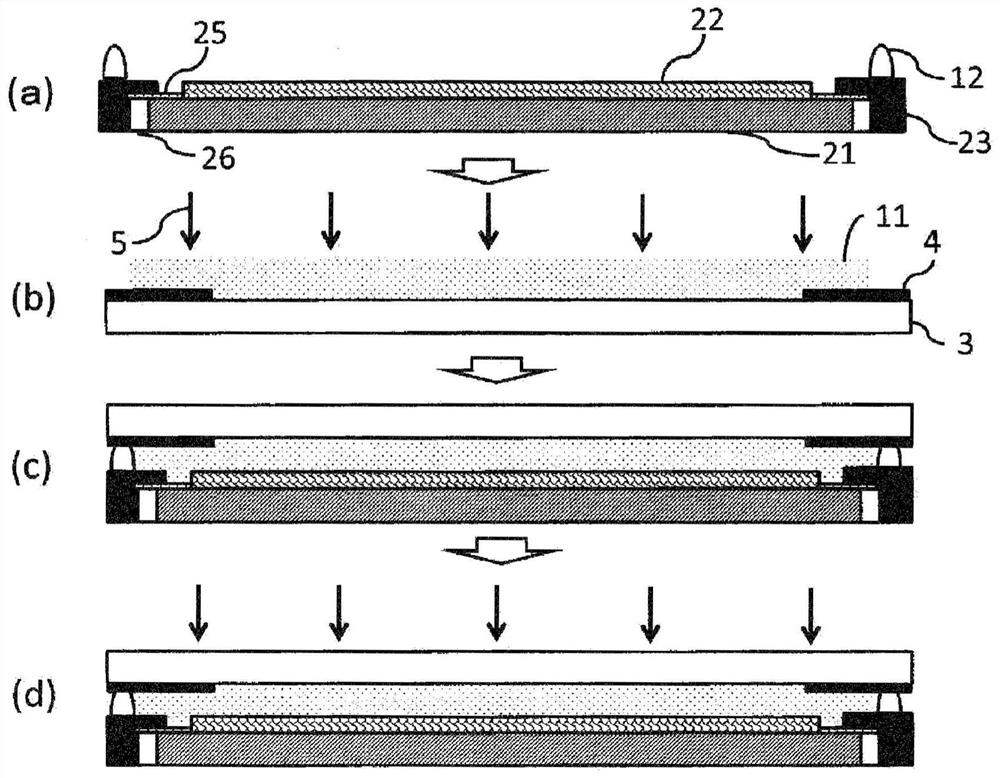
[0056] figure 1 It is a process drawing which shows 1st Embodiment of the manufacturing process of the optical member of this invention.

[0057] This method is a method of obtaining an optical member (image display device) by bonding the liquid crystal display unit 1 and the protective plate 2 together.

[0058] The liquid crystal display unit 1 is a liquid crystal display unit in which a liquid crystal material is sealed between a pair of substrates on which electrodes are formed, and includes a polarizing plate, a driving circuit, a signal input cable, and a backlight unit.

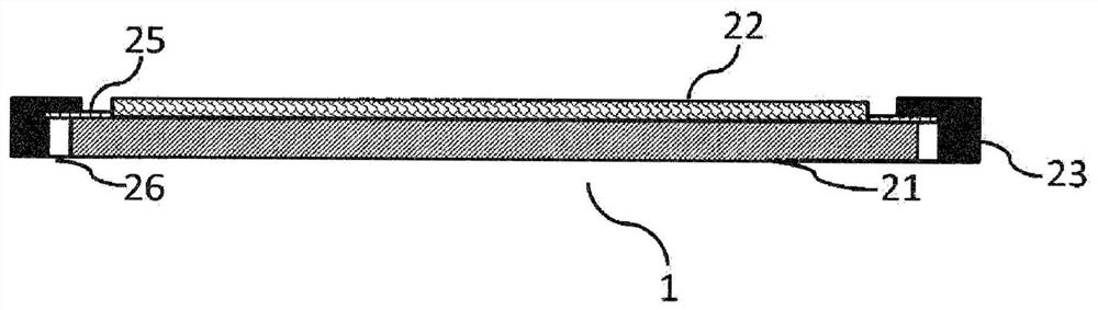
[0059] figure 2 It is a cross-sectional view showing a main part of an example of the liquid crystal display unit 1 . Such as figure 2 As shown, this liquid crystal display unit 1 has a configuration in which a polarizing plate 22 is disposed on a liquid crystal display cell 21 , and a sealing body 23 is disposed on the liquid crystal display cell 21 so as to surround the polarizing plate 22 . He...

no. 2 approach

[0155] The optical member of the present invention can also be produced by the second embodiment modified as follows from the first embodiment.

[0156] [Process A]

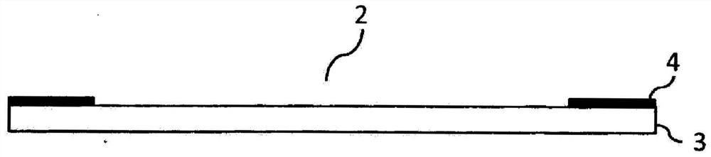
[0157] First, if Figure 5 As shown in (a), the 2nd curable resin composition 12 containing a (meth)acrylate (A) and a photoinitiator (B) is apply|coated on the surface in which the light-shielding part 4 was formed on the guard plate 2.

[0158] [Process B]

[0159] Then, if Figure 5 As shown in (b), the first curable resin composition 11 is coated on the surface of the protective plate 2 on which the light-shielding portion 4 is formed, and then the obtained coating film is irradiated with ultraviolet rays 5 to obtain a The cured product layer exists in the cured portion on the lower side of the layer (the transparent substrate side viewed from the curable resin composition) and the uncured portion on the upper side of the coating layer (the side opposite to the transparent substrate side).

[0160] At this ...

no. 3 approach

[0168] The optical member of the present invention can also be produced by the third embodiment modified as follows on the basis of the first embodiment and the second embodiment.

[0169] [Process A]

[0170] First, if Figure 6 As shown in (a), the second curable resin composition 12 containing (meth)acrylate (A) and photopolymerization initiator (B) is coated on the display surface of the liquid crystal display unit 1 and the protective plate 2. On the surface of the face of the light shielding part 4 .

[0171] [Process B]

[0172] Then, if Figure 6 As shown in (b), the first curable resin composition 11 containing (meth)acrylate (A) and photopolymerization initiator (B) is coated on the display surface of the liquid crystal display unit 1 and the protective plate 2. On the surface of the face of the light shielding part 4 .

[0173] The obtained coating film was irradiated with ultraviolet rays 5 to obtain a cured portion existing on the lower side of the coating fi...


PUM

PropertyMeasurementUnit
thicknessaaaaaaaaaa
thicknessaaaaaaaaaa
thicknessaaaaaaaaaa

Abstract

The present invention provides a method for producing an image display device, a curable resin composition used in the method, and an image display device, the production method of which can obtain an optical display device that does not cause moire and has excellent visibility even when an arbitrary part is pressed. member. As a method of manufacturing an image display device, it includes the steps of defining a coating region of the first curable resin composition with the second curable resin composition, and applying the first curable resin composition to the coating region. step, and a step of curing the first curable resin composition to bond the liquid crystal display unit to the protective plate, and laminating a cured product layer obtained by curing the second curable resin composition on the sealing body. projected area, and not laminated on the projected area of ​​the polarizing plate. It is preferable that the said 1st curable resin composition or the said 2nd curable resin composition contains (meth)acrylate (A) and a photoinitiator (B).

Description

technical field [0001] The present invention relates to a method for producing an image display device (hereinafter also referred to as an optical member) by bonding an optical base material having a light-shielding portion and another optical base material, and a curable resin composition used for the method. Background technique [0002] In recent years, display devices in which a touch panel is bonded to a display screen of a display device such as a liquid crystal display, a plasma display, or an organic electroluminescent (EL) display to enable screen input have been widely used. This touch panel has a structure in which a glass plate or a resin film formed with a transparent electrode is bonded facing each other with a small gap, and a transparent protective plate made of glass or resin is bonded to the touch surface as necessary. [0003] There is a technology of using a double-sided adhesive sheet for bonding a glass plate or film on which a transparent electrode is ...

Claims


Application Information

Patent Timeline
Patent Type & Authority Patents(China)
IPC IPC(8): G02F1/1333C08F2/50G02F1/1335
CPCC08F2/50G02F1/1333G02F1/1335
Inventor 水口贵文本桥隼
Owner NIPPON KAYAKU CO LTD
Why Eureka
Try Eureka