Voltage converter and control method therefor and voltage conversion system

A voltage converter and voltage technology, applied in the circuit field, can solve problems such as energy loss and temperature rise, and achieve the effect of reducing circuit loss and improving energy conversion efficiency

Inactive Publication Date: 2017-05-17
HUAWEI TECH CO LTD
4 Cites 25 Cited by

AI-Extracted Technical Summary

Problems solved by technology

Energy is lost during this transfer, which ...

Method used

By formula (3) it can be seen that, compared with the typical BUCK step-down circuit shown in Figure 1, after the voltage converter provided by the embodiment of the present invention reaches a steady state, the inductor current is reduced to the output current Iout, The loss of the inductance winding DCR is reduced to In addition, in the voltage converter provided by the embodiment of the...

Abstract

The invention discloses a voltage converter and a control method therefor and a voltage conversion system, and energy conversion efficiency of the voltage converter can be improved. The voltage converter comprises an energy storage circuit, wherein the energy storage circuit comprises a first switching element, a second switching element and a first energy storage element; the voltage converter also comprises a third switching element and a second energy storage element, wherein in a first time frame, the first switching element is in a conduction state, the second switching element and the third switching element are in an off state, and a voltage source coupled to the voltage converter charges the first energy storage element and the second energy storage element; in a second time frame after the first time frame, the first switching element is in an off state, and the second switching element and the third switching element are in a conduction state; and the first energy storage element and the second energy storage element discharges to a load which is coupled to the voltage converter.

Application Domain

Technology Topic

Image

  • Voltage converter and control method therefor and voltage conversion system
  • Voltage converter and control method therefor and voltage conversion system
  • Voltage converter and control method therefor and voltage conversion system

Examples

  • Experimental program(1)

Example Embodiment

[0079] The technical solution in this application will be described below in conjunction with the drawings.
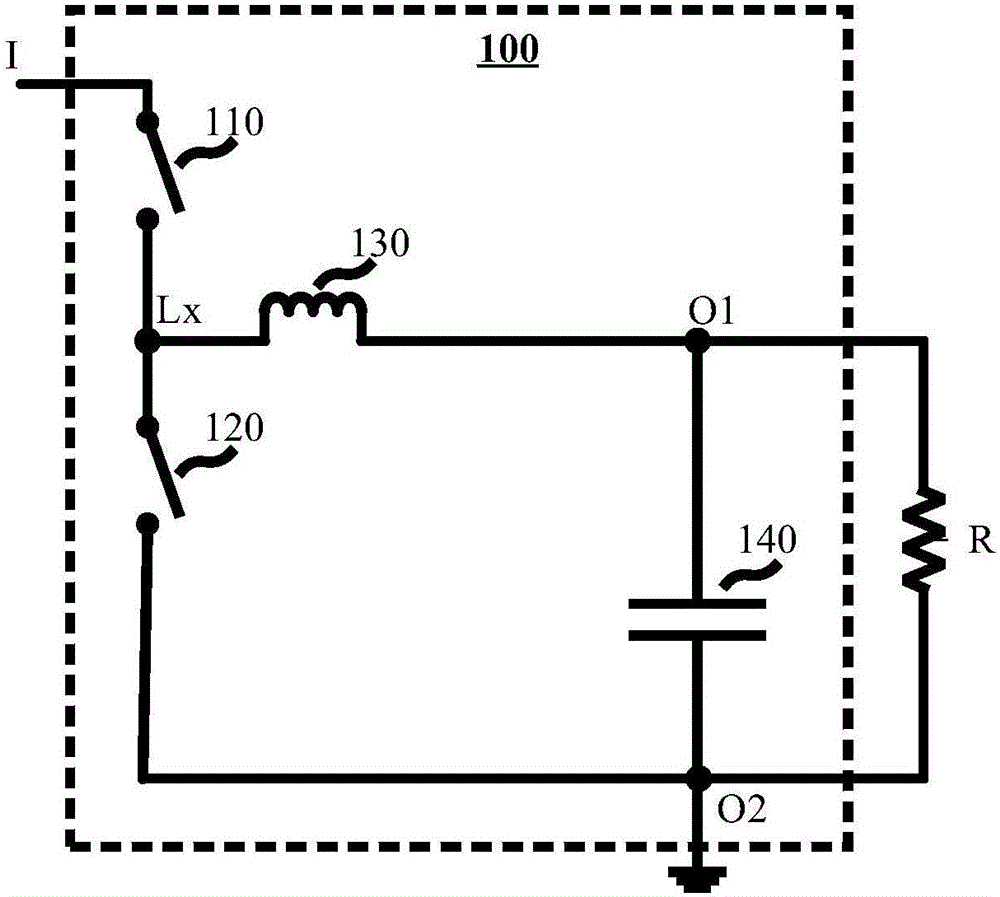
[0080] It should be understood that the embodiments of the present invention can be applied to a DC to DC voltage conversion scenario. Specifically, the embodiment of the present invention can be applied to a buck converter, such as a BUCK circuit, and can also be applied to a boost converter, such as a Boost circuit, which is not limited in the embodiment of the present invention.
[0081] figure 1 A typical BUCK circuit 100 is shown, which can be used to perform step-down conversion of the input voltage and provide it to the load R. Such as figure 1 As shown, the BUCK circuit 100 includes: an input terminal I, a power tube switch 110, a power tube switch 110, an inductor 130, a capacitor 120, and output terminals O1 and O2, wherein the inductor 130 and the capacitor 120 form a filter circuit. Specifically, one end of the power tube switch 110 is connected to the input terminal I of the BUCK circuit 100, the other end of the power tube switch 110 is connected to the terminal Lx, and the terminal Lx is also connected to one end of the inductor 130 and one end of the power tube switch 110. The other end of the device 130 is connected to one end of the capacitor 120, and the other end of the power tube switch 110 is connected to the other end of the capacitor 120. Such as figure 2 As shown, the control signal period T of the BUCK circuit 100 includes two time periods: t ON And t OFF , Where, in the time period t ON , The power tube switch 110 is in the closed state, and the power tube switch 110 is in the open state. At this time, the input voltage V in The terminal LX is connected to the inductor 130, and the inductor 130 is in a state of charging and storing energy. In time period t OFF In this case, the power tube switch 110 is in an off state, the power tube switch 110 is in a closed state, the terminal LX is connected to the ground via the power tube switch 110, and the inductor 130 is in a discharge state.
[0082] When the BUCK circuit 100 reaches a steady state, the following formula is satisfied:
[0083] V out =V in ×D 2 (1)
[0084] I L = I out (2)
[0085] Where V out Is the voltage between the output terminals O1 and O2, that is, the voltage provided by the BUCK circuit 100 to the load, V in Is the input voltage, that is, the voltage of the input terminal I relative to the ground, D 2 Is the duty cycle, equal to t ON And the ratio between T, I L Is the inductor current, I out Is the load current.
[0086] At present, the key constraints of the energy conversion efficiency of the BUCK circuit include: the loss of the inductor winding DCR, which is equal to: DCR×I L 2 , And the parasitic capacitance C at the terminal LX p 的loss, equal to C p ×V iM 2 /2. The embodiment of the present invention provides a voltage converter, which can reduce circuit loss and improve energy conversion efficiency.
[0087] image 3 The voltage converter 200 provided by the embodiment of the present invention is shown. The voltage converter 200 can be used to boost or buck an input voltage provided by a voltage source coupled to the voltage converter 200 and then provide the input voltage to a load coupled to the voltage converter 200. Optionally, the load may be a terminal device, but this embodiment of the present invention does not limit this.
[0088] Such as image 3 As shown, the voltage converter 200 may include an energy storage circuit 210, and the energy storage circuit 210 includes: a first switching element 211, a second switching element 212, and a first energy storage element 213.
[0089] The voltage converter 200 further includes: a first external terminal 220, a third switching element 230, a second energy storage element 240, and a second external terminal 250, wherein,
[0090] The first end of the first switch element 211 is coupled to the first external terminal 220, and the second end of the first switch element 211 is respectively coupled to the first end of the first energy storage element 213 and the second switch element 212 The second end of the second switching element 212 is coupled to the second external terminal 250, and the second end of the first energy storage element 213 is respectively coupled to the first end of the third switching element 230 and the The first end of the second energy storage element 240, the second end of the second energy storage element 240 are coupled to the second external terminal 250, and the second end of the third switch element 230 is grounded.
[0091] In the first time period, the first switching element 211 is in the on state, the second switching element 212 and the third switching element 230 are in the off state, and the voltage source coupled to the voltage converter 200 is the first storage. The energy element 213 and the second energy storage element 240 are charged;
[0092] In a second time period after the first time period, the first switching element 211 is in an off state, the second switching element 212 and the third switching element 230 are in an on state, and the first energy storage element 213 And the second energy storage element 240 respectively discharge to the load coupled to the voltage converter 200.
[0093] The voltage converter 200 may include a first external terminal 220 and a second external terminal 250, wherein one of the first external terminal 220 and the second external terminal 250 can be used to connect to a voltage source, and the other can be used to connect load.
[0094] As an optional embodiment, the first external terminal 220 can be used to connect a load, and the second external terminal 250 can be used to connect a voltage source. In this case, optionally, the voltage converter 200 can be used to connect a voltage source The provided input voltage is boost-converted and then provided to the load, that is, the voltage converter 200 is a boost converter. As another optional embodiment, the first external terminal 220 is used to connect to a voltage source, and the second external terminal 250 is used to connect to a load. At this time, optionally, the voltage converter 200 can be used to provide a voltage source. After performing step-down conversion of the input voltage, the voltage converter 200 is a step-down converter, which is not limited in the embodiment of the present invention.
[0095] Optionally, the first energy storage element 213 and the second energy storage element 240 may be elements capable of storing energy and releasing the stored energy, such as capacitors, inductors, and so on. Optionally, the first energy storage element 213 and the second energy storage element 240 may have different device types. As an optional embodiment, the first energy storage element 213 is a capacitor, and the second energy storage element 240 is an inductor, but the embodiment of the present invention does not limit this.
[0096] Optionally, the number of first energy storage elements 213 included in the voltage converter 200 may be one or more, and the number of second energy storage elements 240 included in the voltage converter 200 may be one or more. The embodiment does not limit this. image 3 It is exemplarily shown that the voltage converter 200 includes a first energy storage element 213 and a second energy storage element 240, but the embodiment of the present invention is not limited thereto.
[0097] In the voltage converter 200, one conversion period (hereinafter referred to as the first conversion period) may include a first time period and a second time period, wherein the second time period may be located after the first time period, and the second time period The length of the period may be equal to or not equal to the length of the first time period, and the embodiment of the present invention does not limit the length of the first time period and the second time period.
[0098] As another optional embodiment, the voltage converter 200 may further include a capacitor C L , Wherein, one end of the capacitor can be connected to the second external terminal 250 of the voltage converter 200, and the other end of the capacitor can be grounded. If the second energy storage element is an inductor, the capacitor C L The filter circuit can be formed with the second energy storage element, but the embodiment of the present invention is not limited thereto.
[0099] Optionally, in the first time period, the first switching element 211 may be in an on state, and the second switching element 212 and the third switching element 230 may both be in an off state, so that the voltage source and the first switching element 211 The first charging loop constituted by the first energy storage element 213, the second energy storage element 240 and the load connected in series is in a conducting state, and the first energy storage element 213 and the second energy storage element 240 are charged and stored.
[0100] Optionally, in the second time period, the first switching element 211 may be in an off state, and the second switching element 212 and the third switching element 230 may be in an on state, so that the first charging circuit is in an off state, The first discharge loop constituted by the first energy storage element 213, the second switching element 212, the load, and the third switching element 230 connected in series in turn is in a conducting state, and the second energy storage element 240, the load and the second The second discharge loop formed by the three switching elements 230 connected in series is in a conducting state, and the first energy storage element 213 and the second energy storage element 240 are discharged and discharged, but the embodiment of the present invention is not limited thereto.
[0101] In the embodiment of the present invention, the first energy storage element can release the stored energy to the load through the first discharge circuit, wherein, optionally, the energy storage element in the first discharge circuit can be the first energy storage The element, that is, the first discharge circuit may not include other energy storage elements except the first energy storage element. The second energy storage element can release the stored energy to the load through the second discharge circuit. Optionally, the first energy storage element and the second energy storage element may be connected in parallel during the second time period, but the embodiment of the present invention is not limited thereto.
[0102] As another optional embodiment, the voltage converter 200 may include: a switching circuit, a first energy storage element, and a second energy storage element.
[0103] Specifically, the switch circuit can be used to turn on the first charging circuit in the first time period, wherein, optionally, in the first charging circuit, the voltage source is connected to the first energy storage element, the second The energy storage element and the load provide energy. At this time, the first energy storage element and the second energy storage element may both be in a charging and energy storage state. Optionally, in the first time period, the voltage source may be connected in series with the first energy storage element, the second energy storage element, and the load, but the embodiment of the present invention is not limited thereto.
[0104] The switch circuit can also be used to disconnect the first charging circuit during the second period of time, and conduct the first discharging circuit and the second discharging circuit, wherein, in the first discharging circuit, the first energy storage element Provide energy to the load, and in the second discharge loop, the second energy storage element provides energy to the load. At this time, the first energy storage element and the second energy storage element may both be in a discharge state.
[0105] The switching circuit may include one or more switching elements. Optionally, the switching circuit may include a first switching element, wherein the first switching element is connected in series in the first charging loop.
[0106] Specifically, in the first charging loop, the first switching element can be connected in series with the first energy storage element, the second energy storage element, and the load. The connection sequence between an energy storage element, the second energy storage element and the load is not limited.
[0107] The first switching element can be used to turn on or off the first charging loop. Optionally, the first switching element may turn on the first charging loop in the first time period, and turn off the first charging loop in the second time period. For example, the first switching element may be in the on state or in the closed state in the first time period, and in the off state in the second time period, but the embodiment of the present invention is not limited thereto.
[0108] As an optional embodiment, in the voltage converter 200, the first terminal of the first switching element may be connected to the first external terminal, and the second terminal of the first switching element may be connected to the first energy storage element. The first end is connected. Optionally, the second end of the first energy storage element may be connected to the first end of the second energy storage element, and the second end of the second energy storage element may be connected to a second external terminal, but the implementation of the present invention Examples are not limited to this.
[0109] Optionally, the switching circuit may include a second switching element, wherein the second switching element may be connected in series in the first discharge loop.
[0110] Specifically, in the first discharging circuit, the second switching element may be connected in series with the first energy storage element and the load, but the embodiment of the present invention is connected to the second switching element, the first energy storage element and the load. The order of connection is not limited.
[0111] Optionally, the second switching element can be used to turn on or off the first discharge loop. Optionally, the second switching element may disconnect the first discharge circuit during the first time period, and turn on the first discharge circuit during the second time period. For example, the second switching element may be in the open state in the first time period, and in the on state or in the closed state in the second time period, but the embodiment of the present invention is not limited thereto.
[0112] As an optional embodiment, in the voltage converter 200, the first end of the second switching element may be connected to the first end of the first energy storage element, and the second end of the second switching element may be connected to The second external terminal of the voltage converter 200 is connected. At this time, optionally, the first end of the first energy storage element may be respectively connected to the second end of the first switching element and the first end of the second switching element, but the embodiment of the present invention is not limited thereto.
[0113] Optionally, the switching circuit may include a third switching element, wherein the third switching element may be connected in series in the second discharge loop.
[0114] Specifically, in the second discharging circuit, the third switching element may be connected in series with the second energy storage element and the load, but the embodiment of the present invention is connected to the third switching element, the second energy storage element and the load. The order of connection is not limited.
[0115] Optionally, the third switching element can be used to turn on or off the second discharge loop. Optionally, the third switching element may disconnect the second discharge circuit in the first time period, and turn on the second discharge circuit in the second time period. For example, the third switching element may be in the open state in the first time period, and in the on state or closed state in the second time period, but the embodiment of the present invention is not limited thereto.
[0116] Optionally, the third switching element may be connected in series in the first discharge loop and the second discharge loop at the same time.
[0117] As an optional embodiment, in the voltage converter 200, the first end of the third switching element may be connected to the second end of the first energy storage element, and the second end of the third switching element may be grounded. At this time, optionally, the second end of the first energy storage element may be respectively connected to the first end of the second energy storage element and the first end of the third switching element, but the embodiment of the present invention is not limited thereto.
[0118] As another alternative embodiment, such as Figure 4 As shown, the energy storage circuit 210 may further include: M third energy storage elements 214 (third energy storage element 1, ..., third energy storage element M), M fourth switching elements 215 (fourth switching element 1...., the fourth switching element M), M fifth switching elements 216 (fifth switching element 1,..., fifth switching element M), and M sixth switching elements 217 (sixth switching element 1,..., The sixth switching element M), where M is an integer greater than or equal to 1.
[0119] Optionally, the third energy storage element 214 may be a device different from the first energy storage element 213 and the second energy storage element 240, or the third energy storage element 214 may also be the same as the first energy storage element. The energy element 213 or the second energy storage element 240 is the same device. As an optional embodiment, the third energy storage element 214 may be a capacitor, but the embodiment of the present invention is not limited thereto.
[0120] Optionally, the first terminal of the fourth switch element 1 may be coupled to the first terminal of the tank circuit 210, that is, the first terminal of the fourth switch element 1 may be coupled to the first external terminal, and the fourth switch element The second end of 1 may be connected to the first end of the third energy storage element 1 and the first end of the fifth switching element 1 respectively. The second terminal of the fifth switch element 1 may be connected to the second external terminal. The second end of the third energy storage element 1 may be connected to the first end of the fourth switching element 2 and the first end of the sixth switching element 1 respectively.
[0121] When i is an integer greater than or equal to 2 and less than or equal to M, the first end of the fourth switching element i can be connected to the second end of the third energy storage element i-1, and the second end of the fourth switching element i The terminals may be respectively connected to the first terminal of the third energy storage element i and the first terminal of the fifth switching element i. The second terminal of the fifth switch element i can be connected to the second external terminal. The second end of the third energy storage element i may be connected to the first end of the sixth switching element i. The second end of the sixth switching element i may be grounded. If i=M, the second end of the third energy storage element i may also be connected to the first end of the first switching element 211.
[0122] Optionally, part or all of the third energy storage elements of the M third energy storage elements 214 may be in a charging and energy storage state during the first time period, and in a discharging and energy-discharging state during the second time period. The embodiment of the invention is not limited to this.
[0123] Optionally, the M fourth switching elements may be connected in series in the first charging loop. The M fourth switching elements can be used to turn on or off the first charging loop. As an optional embodiment, in the first time period, each fourth switching element of the M fourth switching elements may be in a conducting state, so that the first charging loop is in a conducting state. In the second time period, each fourth switching element of the M fourth switching elements may be in an off state, so that the first charging loop is in an off state, but the embodiment of the present invention is not limited thereto.
[0124] Optionally, in the first charging loop, the voltage source may also be used to charge each third energy storage element of the M third energy storage elements. Optionally, in the first charging loop, the M third energy storage elements 214 may be connected in series. In addition, the M third energy storage elements 214 may be further connected to the first external terminal of the voltage converter, The M fourth switching elements, the first switching element 211, the first energy storage element 213, the second energy storage element 240 and the load are connected in series.
[0125] Optionally, in the second time period, each third energy storage element 214 in the discharged state may correspond to a discharge circuit, which is referred to as a third discharge circuit hereinafter. As an optional embodiment, in the second time period, there may be M third discharge circuits, and the M third discharge circuits may correspond to the M third energy storage elements one-to-one, and each third discharge circuit In the loop, the corresponding third energy storage element can release the stored energy to the load, but the embodiment of the present invention is not limited to this.
[0126] Optionally, the M fifth switching elements 214 may correspond to the M third energy storage elements 214 in a one-to-one correspondence, where each fifth switching element 214 may be used to turn on or off the corresponding third energy storage element. The third discharge circuit of the energy element 214. In the third discharge loop, the fifth switching element 214 may be connected in series with the corresponding third energy storage element 214. As an optional embodiment, each fifth switching element 214 may be used to disconnect the third discharge loop including the corresponding third energy storage element 214 in the first time period, and conduct in the second time period including the corresponding The third discharge circuit of the third energy storage element 214, for example, each fifth switching element may be in the off state in the first time period and in the on state in the second time period, but the embodiment of the present invention is not limited to this .
[0127] Optionally, the M sixth switching elements may have a one-to-one correspondence with the M third energy storage elements 214, and each sixth switching element may be used to turn on or turn off the corresponding third energy storage element 214. The third discharge loop. In the third discharge loop, the sixth switching element may be connected in series with the corresponding third energy storage element 214. As an optional embodiment, the sixth switching element may be used to disconnect the third discharge loop including the corresponding third energy storage element 214 in the first time period, and turn on the third discharge loop including the corresponding third energy storage element 214 in the second time period. The third discharge circuit of the energy element 214, for example, each sixth switching element may be in the off state in the first time period and in the on state in the second time period, but the embodiment of the present invention is not limited thereto.
[0128] As an optional embodiment, in the second time period, the third discharge loop formed by the third energy storage element i, the fifth switching element i, the sixth switching element i and the load connected in series is turned on, and the third energy storage element The energy element i provides energy to the load, but the embodiment of the present invention is not limited thereto.
[0129] It should be understood that in Figure 4 In the example shown, the tank circuit 210 includes M fourth switching elements, M fifth switching elements, and M sixth switching elements. However, the embodiment of the present invention does not limit the number of the fourth switching element, the fifth switching element, and the sixth switching element included in the tank circuit 210.
[0130] As another optional embodiment, the voltage converter 200 may further include a seventh switching element 260, and the seventh switching element 260 may be used to make the energy storage element in the energy storage circuit 210 (for example, the first energy storage element 213) , Or the first energy storage element 213 and the M third energy storage elements 214) are in a working state or a bypass state. Optionally, when the energy storage element in the energy storage circuit 210 is in a working state, the voltage converter 200 may work in the first working mode. In the first working mode, the working principle of the voltage converter 200 can refer to the description of the voltage converter 200 above. Optionally, when the energy storage element in the energy storage circuit 210 is in a bypass state, the voltage converter 200 may work in the second working mode.
[0131] If the voltage converter 200 is in the second working mode, the second charging circuit can be in a conducting state during the third time period, wherein, in the second charging circuit, the voltage source is directed to the second energy storage element 240 and the load provide energy, and the second energy storage element charges and stores energy. At this time, the second charging loop may not include the energy storage element in the energy storage circuit 210. Optionally, in a fourth time period after the third time period, the second charging loop may be in an off state, the second discharging loop may be in an on state, and the second energy storage element 240 may provide the load to the load. Energy, but the embodiment of the present invention is not limited to this.
[0132] Optionally, in the second working mode, the voltage converter 200 may have a second conversion period, and the second conversion period may include the third time period and the fourth time period after the third time period. Optionally, the second conversion period and the first conversion period may be the same or different, the length of the first time period and the third time period may be the same or different, and the length of the second time period and the fourth time period may be the same Or different, the embodiment of the present invention does not limit this.
[0133] As an optional embodiment, such as Figure 5 As shown, the first end of the seventh switch element 260 can be connected to the first external terminal, and the second end of the seventh switch element 260 can be connected to the second end of the first energy storage element 213 and the second storage element 213. The first end of the energy element 240 and the first end of the third switch element 230 are connected, but the embodiment of the present invention is not limited thereto.
[0134] Optionally, in the second operating mode, the first switching element 211 and the second switching element 212 may always be kept in an off state.
[0135] In the third time period, the seventh switching element 260 may be in an on state, and the third switching element 230 may be in an off state, so that the voltage source, the seventh switching element 260, the second energy storage element 240 and the load The second charging loop formed by sequentially connecting in series is in a conducting state, and the second energy storage element 240 charges and stores energy.
[0136] In the fourth time period, the seventh switching element 260 may be in the off state, and the third switching element 230 may be in the on state, so that the second charging loop is in the off state, and the second energy storage element 240, The second discharge circuit formed by the load and the third switching element 230 is in a conducting state, and the second energy storage element 240 discharges energy, but the embodiment of the present invention is not limited thereto.
[0137] When the voltage converter 200 reaches a steady state in the second working mode, the above equations (1) and (2) can be satisfied, but the embodiment of the present invention is not limited thereto.
[0138] Optionally, the switching element in the embodiment of the present invention may be a device such as a semiconductor MOSFET transistor, a semiconductor rectifier or a semiconductor diode, etc., which is not limited in the embodiment of the present invention.
[0139] As another optional embodiment, the voltage converter 200 may further include: a controller, configured to send a driving signal to each switching element in the voltage converter 200 to control the state of each switching element. Wherein, optionally, the controller may be specifically a control circuit or a control chip, which is not limited in the embodiment of the present invention.
[0140] Image 6 An example of a voltage converter 300 provided by an embodiment of the present invention is shown. Here, it is assumed that the voltage converter 300 is a buck converter. Such as Image 6 As shown, the voltage converter 300 includes: a first external terminal 320 for connecting a voltage source, a power tube switch 311, a power tube switch 312, a capacitor 313, a power tube switch 330, an inductor 340, a capacitor 370, and a The second external terminal 350 of the load, wherein the inductor 340 and the capacitor 370 constitute a filter circuit.
[0141] Specifically, in the voltage converter 300, the first energy storage element is a capacitor C F , The second energy storage element is an inductor L, and each switching element is a power tube switch.
[0142] Optionally, in the first time period, the power tube switch 311 may be in the on state, and the power tube switch 312 and the power tube switch 330 may be in the off state, so that the voltage source and the power tube switch coupled to the first external terminal The first charging loop formed by the series connection of the switch 311, the capacitor 313, the inductor 340, and the load R coupled to the second external terminal is in a conducting state, and the capacitor 313 and the inductor 340 are both in a charging and energy storage state. Optionally, in the second time period, the power tube switch 311 may be in the off state, and the power tube switch 312 and the power tube switch 330 are in the on state, so that the first charging circuit is in the off state, and the capacitor 313 The first discharge circuit formed by the series connection of the power tube switch 312, the load R and the power tube switch 330 is in a conducting state. The capacitor 313 releases the stored energy through the first discharge circuit, and the inductor 340, the load R and The second discharge circuit formed by the series connection of the power tube switches 330 is in a conducting state, and the inductor 340 releases the stored energy through the second discharge circuit.
[0143] In addition, Image 6 Illustratively shows that the voltage converter 300 includes a capacitor C F Optionally, the voltage converter 300 may include N capacitors C F , The N capacitors C may all be in a charged state in the first time period, respectively correspond to a discharge circuit in the second time period, and release the stored energy to the load through the corresponding discharge circuit, where, optionally, N may be equal to M+1, that is, the above M third energy storage elements can all be capacitors C F. In this way, when the circuit of the voltage converter 300 reaches a steady state, the following relationship can be satisfied:
[0144]
[0145]
[0146] Where V out Is the voltage of the output load, that is, the output voltage of the voltage converter, V in Is the voltage source, that is, the input voltage provided by the voltage source to the voltage converter, D 1 Is the duty cycle, equal to the ratio between the first time period and the first conversion period, I L Is the inductor current, I out Is the output current.
[0147] From equation (3), we can see that with figure 1 Compared with the typical BUCK step-down circuit shown, the voltage converter provided by the embodiment of the present invention reduces the inductor current to the output current I after the circuit reaches a steady state. out of In this way, the loss of the inductor winding DCR is reduced to In addition, in the voltage converter provided by the embodiment of the present invention, the voltage swing at the terminal LX is reduced to V in -N×V out , In this way, the parasitic capacitance loss at the terminal LX is reduced to In this way, with figure 1 Compared with the typical BUCK step-down circuit shown, the energy conversion efficiency of the voltage converter provided by the embodiment of the present invention is effectively improved by reducing the circuit loss.
[0148] An embodiment of the present invention also provides a voltage conversion system, which may include any voltage converter described above, and a voltage source and load coupled to the voltage converter. The specific structure and working principle can be referred to the above description, for the sake of brevity, it will not be repeated here.
[0149] Combine the above Figure 2 to Figure 6 The voltage converter provided by the embodiment of the present invention is described in detail, and the following combination Figure 7 The control method of the voltage converter provided by the embodiment of the present invention is described in detail.
[0150] Figure 7 The voltage converter control method 400 provided by the embodiment of the present invention is shown. Optionally, the voltage converter can be any voltage converter 200 described above, but the embodiment of the present invention does not do this. limited. The method 400 includes:
[0151] S410. Send a first driving signal to the first switching element, and send a second driving signal to the second switching element and the third switching element, so that the voltage source coupled to the voltage converter is at the first time period. The first energy storage element and the second energy storage element are charged, wherein the first driving signal is used to control the first switching element to be in a conducting state during the first time period, and to charge the second switching element and the third The second driving signal sent by the switching element is respectively used to control the second switching element and the third switching element to be in an off state during the first time period;
[0152] S420. Send a third drive signal to the first switch element, and send a fourth drive signal to the second switch element and the third switch element, so that the first energy storage element and the second energy storage element are located in the A second time period after the first time period is respectively discharged to the load coupled to the voltage converter, wherein the third drive signal is used to control the first switching element to be in an off state during the second time period, and to The fourth driving signal sent by the second switching element and the third switching element is respectively used to control the second switching element and the third switching element to be in a conducting state during the second time period.
[0153] Optionally, in S410 and S420, the controller may send driving signals to each switching element at the same time or in any sequence. In addition, S410 and S420 may be executed simultaneously or S410 may be executed before S420, which is not limited in the embodiment of the present invention.
[0154] Optionally, the first driving signal and the second driving signal may be the same or different signals, and the third driving signal and the fourth driving signal may be the same or different signals, which is not limited in the embodiment of the present invention .
[0155] Optionally, the method 400 further includes: the controller sends a fifth control signal to the seventh switching element, where the fifth control signal is used to control the seventh switching element to be in both the first time period and the second time period. Disconnected state.
[0156] Optionally, the method 400 further includes:
[0157] The controller sends a sixth control signal to the seventh switching element, and sends a seventh switching signal to the first switching element, the second switching element, and the third switching element, so that the voltage source is in the third time period Charge the second energy storage element, wherein the sixth control signal is used to control the seventh switching element to be in the on state during the third period of time, and to charge the first switching element, the second switching element, and the first switching element; The seventh switching signal sent by the three switching elements is respectively used to control the first switching element, the second switching element, and the third switching element to be in an off state during the third time period;
[0158] The controller sends an eighth control signal to the seventh switching element, the first switching element, and the second switching element, and sends a ninth control signal to the third switching element, so that the second energy storage element is located at the Discharge to the load in a fourth time period after the third time period, wherein the eighth control signal sent to the seventh switching element, the first switching element, and the second switching element are respectively used to control the seventh switch The element, the first switching element, and the second switching element are in the off state during the fourth time period, and the ninth control signal is used to control the third switching element to be in the on state during the fourth time period.
[0159] As another optional embodiment, the control method 400 includes: sending a first driving signal to a switching circuit in the voltage converter, so that the switching circuit turns on the first charging loop in the first time period, wherein In a charging loop, a voltage source coupled to the voltage converter provides energy to the first energy storage element, the second energy storage element, and the load; and sends a second drive signal to the switch circuit to make the switch The circuit disconnects the first charging circuit in a second time period after the first time period, and conducts the first discharging circuit and the second discharging circuit, wherein, in the first discharging circuit, the first storage circuit is The energy element provides energy to the load, and in the second discharge loop, the second energy storage element provides energy to the load.
[0160] Optionally, the first driving signal and the second driving signal may be sent in the first time period and the second time period respectively, or may be sent simultaneously or in any order, which is not done in this embodiment of the present invention. limited.
[0161] Optionally, the first driving signal may be used to control the first switching element to be in the on state during the first time period, and the second driving signal may be used to control the first switching element to be in the off state during the second time period , But the embodiment of the present invention is not limited to this.
[0162] Optionally, the first driving signal may be used to control the second switching element to be in the off state during the first time period, and the second driving signal may be used to control the second switching element to be in the on state during the second time period , But the embodiment of the present invention is not limited to this.
[0163] Optionally, the first driving signal may be used to control the third switching element to be in the off state during the first time period, and the second driving signal may be used to control the third switching element to be in the on state during the second time period , But the embodiment of the present invention is not limited to this.
[0164] Optionally, before sending the first driving signal and the second driving signal to the switch circuit, the method 400 may further include:
[0165] The third driving signal is sent to the seventh switching element, so that the seventh switching element is in an off state.
[0166] Optionally, the method 400 may further include: sending a fourth driving signal to the seventh switching element, so that the seventh switching element bypasses the first energy storage element.
[0167] Optionally, the method may further include: sending a fifth driving signal to the switching circuit, so that the switching circuit turns on the second charging loop in the third time period, and sending a sixth driving signal to the switching circuit to So that the switch circuit disconnects the second charging circuit and turns on the second discharging circuit in a fourth time period after the third time period, wherein, in the second charging circuit, a voltage source flows to the second The energy storage element and the load provide energy.
[0168] In an optional example, those skilled in the art can understand that the method 400 may be executed by the controller in the above-mentioned embodiment, and to avoid repetition, it will not be repeated here.
[0169] It should be understood that the size of the sequence numbers of the foregoing processes does not mean the order of execution. The execution order of the processes should be determined by their functions and internal logic, and should not constitute any limitation on the implementation process of the embodiments of the present invention.
[0170] It should also be understood that, in the embodiments of the present invention, the same elements correspond to similar reference numerals. In addition, the above description of the embodiments of the present invention focuses on emphasizing the differences between the various embodiments, and the unmentioned similarities or similarities can be referred to each other, and for the sake of brevity, details are not repeated here.
[0171] It should also be understood that, in this context, the connection between A and B may mean that A and B are directly connected, or A and B are indirectly connected, for example, A is connected to B through one or more elements, which is not limited in the embodiment of the present invention.
[0172] In addition, the terms "system" and "network" in this article are often used interchangeably in this article. The term "and/or" in this text is only an association relationship that describes the associated objects, which means that there can be three relationships, for example, A and/or B, which can mean: A alone exists, A and B exist at the same time, exist alone B these three situations. In addition, the character "/" in this text generally indicates that the associated objects before and after are in an "or" relationship.
[0173] A person of ordinary skill in the art may realize that the units and algorithm steps of the examples described in combination with the embodiments disclosed herein can be implemented by electronic hardware or a combination of computer software and electronic hardware. Whether these functions are executed by hardware or software depends on the specific application and design constraints of the technical solution. Professionals and technicians can use different methods for each specific application to implement the described functions, but such implementation should not be considered as going beyond the scope of the present invention.
[0174] Those skilled in the art can clearly understand that, for convenience and concise description, the specific working process of the above-described system, device, and unit can refer to the corresponding process in the foregoing method embodiment, and details are not described herein again.
[0175] In the several embodiments provided in this application, it should be understood that the disclosed system, device, and method may be implemented in other ways. For example, the device embodiments described above are merely illustrative. For example, the division of the units is only a logical function division, and there may be other divisions in actual implementation, for example, multiple units or components may be combined or It can be integrated into another system, or some features can be ignored or not implemented. In addition, the displayed or discussed mutual coupling or direct coupling or communication connection may be indirect coupling or communication connection through some interfaces, devices or units, and may be in electrical, mechanical or other forms.
[0176] The units described as separate components may or may not be physically separated, and the components displayed as units may or may not be physical units, that is, they may be located in one place, or they may be distributed on multiple network units. Some or all of the units may be selected according to actual needs to achieve the objectives of the solutions of the embodiments.
[0177] In addition, the functional units in each embodiment of the present invention may be integrated into one processing unit, or each unit may exist alone physically, or two or more units may be integrated into one unit.
[0178] If the function is implemented in the form of a software functional unit and sold or used as an independent product, it can be stored in a computer readable storage medium. Based on this understanding, the technical solution of the present invention essentially or the part that contributes to the existing technology or the part of the technical solution can be embodied in the form of a software product, and the computer software product is stored in a storage medium, including Several instructions are used to make a computer device (which may be a personal computer, a server, or a network device, etc.) execute all or part of the steps of the methods described in the various embodiments of the present invention. The aforementioned storage media include: U disk, mobile hard disk, read-only memory (Read-Only Memory, ROM), random access memory (Random Access Memory, RAM), magnetic disk or optical disk and other media that can store program code .
[0179] The above are only specific implementations of this application, but the scope of protection of this application is not limited to this. Any person skilled in the art can easily think of changes or substitutions within the technical scope disclosed in this application. Should be covered within the scope of protection of this application. Therefore, the protection scope of this application shall be subject to the protection scope of the claims.

PUM

no PUM

Description & Claims & Application Information

We can also present the details of the Description, Claims and Application information to help users get a comprehensive understanding of the technical details of the patent, such as background art, summary of invention, brief description of drawings, description of embodiments, and other original content. On the other hand, users can also determine the specific scope of protection of the technology through the list of claims; as well as understand the changes in the life cycle of the technology with the presentation of the patent timeline. Login to view more.

Similar technology patents

Voltage output circuit, driving circuit and switching power supply

ActiveCN109673095AReduce the number of turns and the radius of the wireReduce circuit lossElectrical apparatusElectric lighting sourcesLight sourceHigh pressure
Owner:FUJIAN RAYNEN TECH

Printed circuit board and electronic equipment

PendingCN112601345AReduce circuit lossIncrease coupling areaPrinted circuit detailsGrounding gridPrinted circuit board
Owner:SHENZHEN K FREE WIRELESS INFORMATION TECH

Driving circuit and switching power supply

ActiveCN109526128AReduce the number of turns and the radius of the wireReduce circuit lossElectrical apparatusElectric lighting sourcesLight sourcePower flow
Owner:FUJIAN RAYNEN TECH

Classification and recommendation of technical efficacy words

  • Reduce circuit loss
  • Improve energy conversion efficiency

Printed circuit board and electronic equipment

PendingCN112601345AReduce circuit lossIncrease coupling areaPrinted circuit detailsGrounding gridPrinted circuit board
Owner:SHENZHEN K FREE WIRELESS INFORMATION TECH
Why Eureka
Try Eureka