Supercharge Your Innovation With Domain-Expert AI Agents!

The pixel structure of cmos image sensor, cmos image sensor and its imaging method

An image sensor and pixel structure technology, applied in image communication, electrical components, color TV components and other directions, can solve the problems of reducing pixel charge transfer efficiency, complex image sensor structure, image sensor performance impact, etc. Clock frequency, good adaptability, the effect of improving imaging performance

Active Publication Date: 2019-06-07
NORTHWEST INST OF NUCLEAR TECH
View PDF9 Cites 0 Cited by
  • Summary
  • Abstract
  • Description
  • Claims
  • Application Information

AI Technical Summary

Problems solved by technology

At present, ISIS is mainly researched and applied to CCD image sensors, and it is relatively difficult to realize ISIS under the CMOS process.
figure 2 It is an ISIS planar structure diagram with a linear CCD storage structure. This in-situ image sensor structure is relatively complex, and a higher transfer clock frequency will reduce the transfer efficiency of pixel charges, thereby affecting the performance of the image sensor; and the chip passes through the gate. The ultra-high-speed opening and closing of the valve electrode is used to realize charge collection. Since the entire chip generally exceeds 1 million pixels, each pixel includes interconnected resistors and capacitors. When the gate valve electrode is opened, a large current will be formed inside. , which poses a great challenge to the design of the image sensor and the stability of the imaging

Method used


Image

  • The pixel structure of cmos image sensor, cmos image sensor and its imaging method
  • The pixel structure of cmos image sensor, cmos image sensor and its imaging method
  • The pixel structure of cmos image sensor, cmos image sensor and its imaging method

Examples


Embodiment Construction

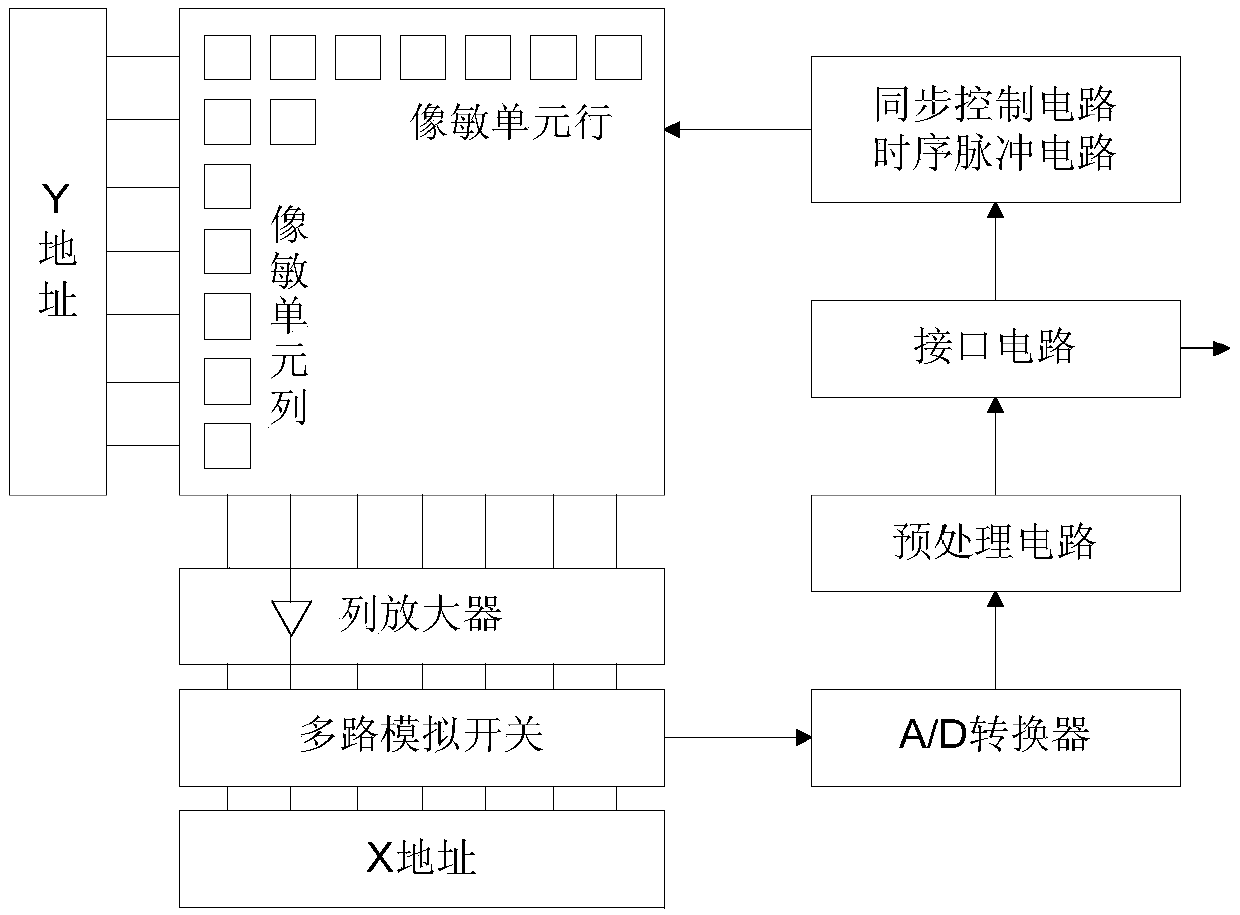
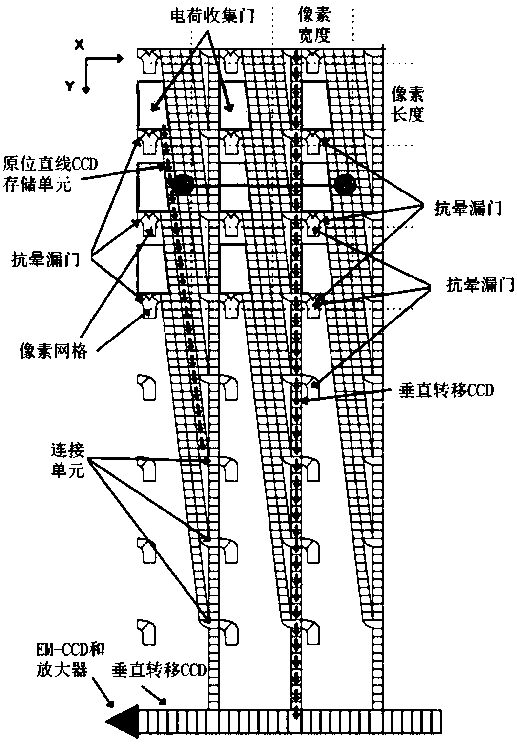
[0036] The pixel structure of the CMOS image sensor provided by the present invention is characterized in that each includes a photodiode with N output ports, N storage devices, N gate valves and N pixel readout circuits; N storage devices The input ends of the photodiode are respectively connected to the N output ports of the photodiode through N gate valves; the output ends of the N memory devices are respectively connected to the N pixel readout circuits. Each storage device is composed of a plurality of CCD storage units.

[0037] In practical applications, the size and arrangement of the N storage devices are flexibly designed according to the spatial positions in the CMOS image sensor chip.

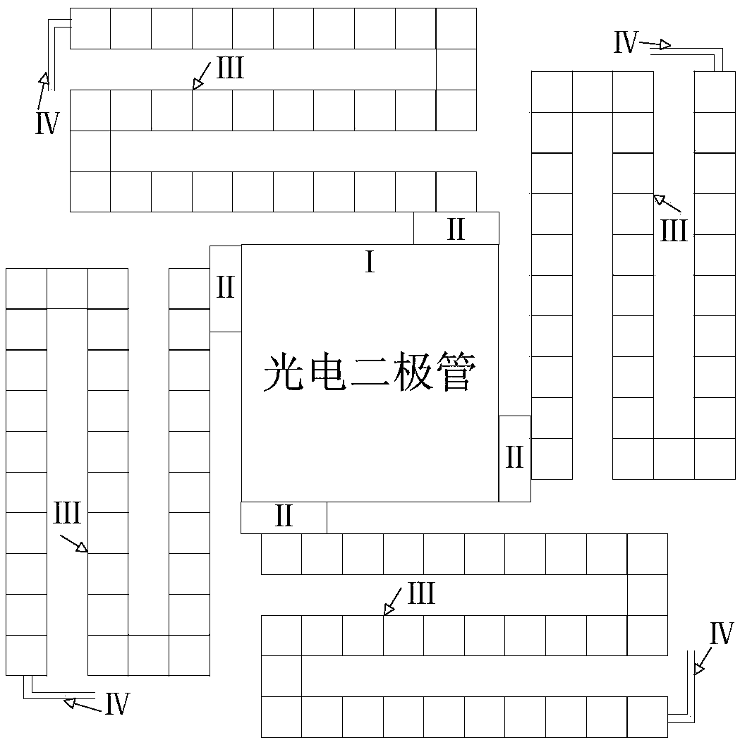
[0038] image 3 Shown is the structure model when the pixel structure of the CMOS image sensor provided by the present invention is four ports. Among them, the area I is a photodiode, the area II is a gate valve structure connecting the photodiode and the storage area (that is, th...


PUM


Abstract

In order to enable the CMOS image sensor to achieve ultra-high time-resolution continuous imaging, the present invention provides a pixel structure of the CMOS image sensor, each pixel includes a photodiode with N output ports, N storage devices, N gate valve and N picture element readout circuits; the input ends of the N storage devices are respectively connected to the N output ports of the photodiode through the N gate valves; the output ports of the N storage devices are respectively connected to the The N pixel readout circuits are connected.

Description

technical field [0001] The invention belongs to the field of optical image sensors, and in particular relates to a pixel structure of a CMOS image sensor, a CMOS image sensor and an imaging method thereof. Background technique [0002] Ultra-high-speed imaging systems are of great significance to the study of fast physical processes, and image sensor chips are even more crucial as the core components of imaging systems. There are two main types of traditional image sensors: CCD image sensors and CMOS image sensors. Compared with CCD devices, the advantage of CMOS image sensors is that more high-speed ADCs can be integrated on-chip, so that the data output speed of the image sensor is very high. The traditional CMOS image sensor structure adopts a bidirectional continuous output pixel layout, such as figure 1 As shown, the principle is: the optical signal is converted into an electrical signal in the photosensitive area, and selected by the address decoder in the X and Y di...

Claims


Application Information

Patent Timeline
Patent Type & Authority Patents(China)
IPC IPC(8): H04N5/374H04N5/3745
CPCH04N25/771H04N25/76H04N25/77
Inventor 杨少华刘璐严明李刚郭明安李斌康甘泉
Owner NORTHWEST INST OF NUCLEAR TECH
Features
  • R&D
  • Intellectual Property
  • Life Sciences
  • Materials
  • Tech Scout
  • Unparalleled Data Quality
  • Higher Quality Content
  • 60% Fewer Hallucinations
Learn More