Pixel unit structure realizing three conversion gains

A technology of pixel unit and conversion gain, applied in the field of pixel unit structure of CMOS image sensor, can solve the problems such as image fineness affecting the imaging range of pixel unit, lack of intermediate state conversion gain curve, etc., and achieve high sensitivity and large dynamic range. Effect

Active Publication Date: 2017-05-17
SHANGHAI INTEGRATED CIRCUIT RES & DEV CENT +1
View PDF7 Cites 0 Cited by
  • Summary
  • Abstract
  • Description
  • Claims
  • Application Information

AI Technical Summary

Problems solved by technology

[0011] However, the conventional double conversion gain pixel unit has only two conversion gain modes, high and low, and lacks an intermediate conversion gain curve, which affects the range of use of pixel unit imaging and the fineness of imaging.

Method used


Image

  • Pixel unit structure realizing three conversion gains
  • Pixel unit structure realizing three conversion gains
  • Pixel unit structure realizing three conversion gains

Examples


Embodiment Construction

[0031] The specific embodiment of the present invention will be further described in detail below in conjunction with the accompanying drawings.

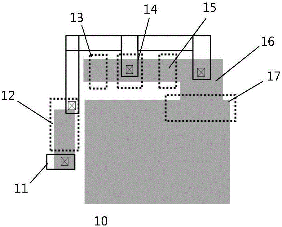
[0032] It should be noted that, in the following specific embodiments, when describing the embodiments of the present invention in detail, in order to clearly show the structure of the present invention for the convenience of description, the structures in the drawings are not drawn according to the general scale, and are drawn Partial magnification, deformation and simplification are included, therefore, it should be avoided to be interpreted as a limitation of the present invention.

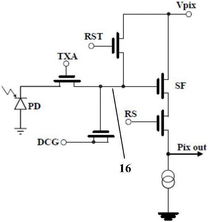
[0033] In the following specific embodiments of the present invention, please refer to Figure 4 , Figure 4 It is a schematic diagram of the circuit structure of a pixel unit structure realizing three conversion gains in a preferred embodiment of the present invention. Such as Figure 4 As shown, a pixel unit structure for realizing three convers...


PUM


Abstract

The invention discloses a pixel unit structure realizing three conversion gains. The pixel unit structure at least comprises a photodiode, a transmission tube, a reset tube, a source electrode following tube and a gain control tube. A drain electrode of the transmission tube, a grid electrode of the source electrode following tube and a source electrode of the reset tube are jointly connected to a suspension drain electrode. The gain control tube and the suspension drain electrode are in parallel arrangement, and the gain control tube comprises first and second control ends. By different voltage biases on the first and second control ends under different illumination conditions, three different capacitance values of the suspension drain electrode are achieved, and accordingly switching of a pixel unit among the three conversion gains is realized, high-quality image output is obtained, and requirements of a CMOS (complementary metal oxide semiconductor) image sensor on high sensitivity and large dynamic range are met.

Description

technical field [0001] The present invention relates to the technical field of image sensors, and more particularly relates to a CMOS image sensor pixel unit structure capable of realizing three conversion gains. Background technique [0002] Generally, an image sensor refers to a device that converts an optical signal into an electrical signal. According to different manufacturing processes and working principles, image sensors can be further divided into charge-coupled device (CCD) and complementary metal-oxide semiconductor (CMOS) image sensor chips. [0003] Compared with traditional CCD sensors, CMOS image sensors have the characteristics of low power consumption, low cost and compatibility with CMOS technology, so they are more and more widely used. CMOS image sensors are now not only used in consumer electronics, such as miniature digital cameras (DSC), mobile phone cameras, video cameras and digital single-lens reflex (DSLR), but also in automotive electronics, moni...

Claims


Application Information

Patent Timeline
Patent Type & Authority Applications(China)
IPC IPC(8): H04N5/374H04N5/3745
CPCH04N25/77H04N25/76
Inventor 顾学强周伟范春晖王言虹
Owner SHANGHAI INTEGRATED CIRCUIT RES & DEV CENT
Why Eureka
Try Eureka