Fingerprint identification device and mobile terminal
A fingerprint identification and fingerprint technology, applied in the field of fingerprint identification, can solve the problems of reducing the security of mobile terminals, cracking, and the inability to judge fake fingerprints, etc., and achieve the effects of reducing the risk of fake fingerprint cracking, low cost, and simple structure
- Summary
- Abstract
- Description
- Claims
- Application Information
AI Technical Summary
Problems solved by technology
Method used
Image

Examples
Embodiment 1
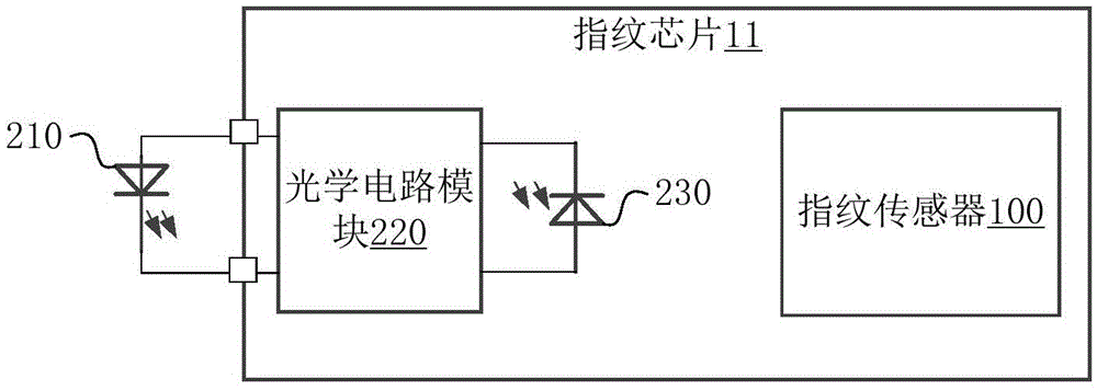
[0086] Such as image 3 As shown, in this embodiment, the optical circuit module 220, the photoelectric converter 230 and the fingerprint sensor 100 are integrated into one chip, which is called the fingerprint chip 11; the light emitter 210 is an independent device, which can be single or multiple. The fingerprint chip 11 can be packaged together with the light emitter 210 to form a fingerprint encapsulation sheet; or, the fingerprint chip 11 is packaged separately to form a fingerprint encapsulation sheet, and the light emitter 210 is placed outside the fingerprint encapsulation sheet.
[0087] Such as Figure 4 , Figure 5 Shown is the first scheme of this embodiment, wherein, Figure 4 main view, Figure 5 for Figure 4 The sectional view of A-A in the middle (subsequent sectional views are all sectional views along A-A, for the sake of simplification, they are not marked one by one in the figure). This scheme is that the fingerprint chip 11 and the light emitter 210 ...
Embodiment 2
[0100] Such as Figure 25 As shown, in this embodiment, the optical circuit module 220 and the fingerprint sensor 100 are integrated into one chip, which is called the fingerprint chip 11; the light emitter 210 and the photoelectric converter 230 are independent devices. The fingerprint chip 11 can be packaged together with the light emitter 210 and the photoelectric converter 230 to form the fingerprint encapsulation sheet 10. The structural layout of this integrated mode is similar to the situation of the first solution in Embodiment 1, and will not be described in detail here; The chip 11 can also be packaged together with the photoelectric converter 230 to form the fingerprint encapsulation sheet 10, and the light emitter 210 is placed outside the fingerprint encapsulation sheet 10. The structural layout of this integration mode is similar to the situation of the second solution in the first embodiment , will not be repeated here; the fingerprint chip 11 can also constitut...
Embodiment 3
[0105] Such as Figure 34 As shown, in this embodiment, the fingerprint sensor 100 is independently integrated into a chip, which is the fingerprint chip 11, and the optical circuit module 220 is electrically connected to the fingerprint sensor 100 through a data interface, such as a serial peripheral interface (Serial Peripheral Interface) , SPI for short) interface, I2C (Inter-Integrated Circuit) bus interface, Universal Asynchronous Receiver / Transmitter (UART for short) interface, Universal Serial Bus (Universal Serial Bus, USB for short) interface, etc. Any two or three of the light emitter 210, the photoelectric converter 230, and the optical circuit module 220 can be combined into an integrated chip or an overall package, or can be a single independent device.
[0106] Such as Figure 35 As shown, the fingerprint chip 11 is individually packaged into a fingerprint package 10, and the optical circuit module 220, photoelectric converter 230, and light emitter 210 are inte...
PUM
 Abstract
Description
Claims
Application Information
 - R&D
- Intellectual Property
- Life Sciences
- Materials
- Tech Scout
- Unparalleled Data Quality
- Higher Quality Content
- 60% Fewer Hallucinations
Browse by: Latest US Patents, China's latest patents, Technical Efficacy Thesaurus, Application Domain, Technology Topic, Popular Technical Reports.
© 2025 PatSnap. All rights reserved.Legal|Privacy policy|Modern Slavery Act Transparency Statement|Sitemap|About US| Contact US: help@patsnap.com