Method for efficiently and controllably processing large-area silicon micro-nano structure

A large-area, silicon micro-nano technology, applied in the field of femtosecond laser applications, can solve the problems of low processing efficiency and high cost, and achieve the effects of improving processing efficiency, facilitating operation and control, and reducing costs

Inactive Publication Date: 2017-05-31
BEIJING INSTITUTE OF TECHNOLOGYGY
View PDF6 Cites 20 Cited by
  • Summary
  • Abstract
  • Description
  • Claims
  • Application Information

AI Technical Summary

Problems solved by technology

[0004] The purpose of the present invention is to solve the problem of low processing efficiency and high cost of existing high-quality, high-uniform large-area silicon nano-dot arrays

Method used


Image

  • Method for efficiently and controllably processing large-area silicon micro-nano structure
  • Method for efficiently and controllably processing large-area silicon micro-nano structure

Examples


Embodiment

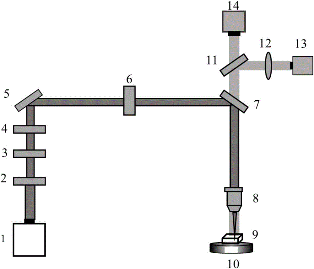
[0030] The femtosecond laser system in this embodiment adopts the laser produced by American Spectra Physics Company, the laser center wavelength is 800nm, the pulse width is 35fs, the repetition frequency is adjustable at 1KHz, the single pulse maximum energy is 3mJ, and the light intensity distribution is Gaussian , linearly polarized.

[0031] The processing material 9 is N-type non-doped single crystal silicon with crystal orientation 100, and its size is 10mm×10mm×1mm. Of course, those skilled in the art know that the actual processed object is not limited to single crystal silicon, it can be any other substance whose chemical properties can be changed by laser irradiation.

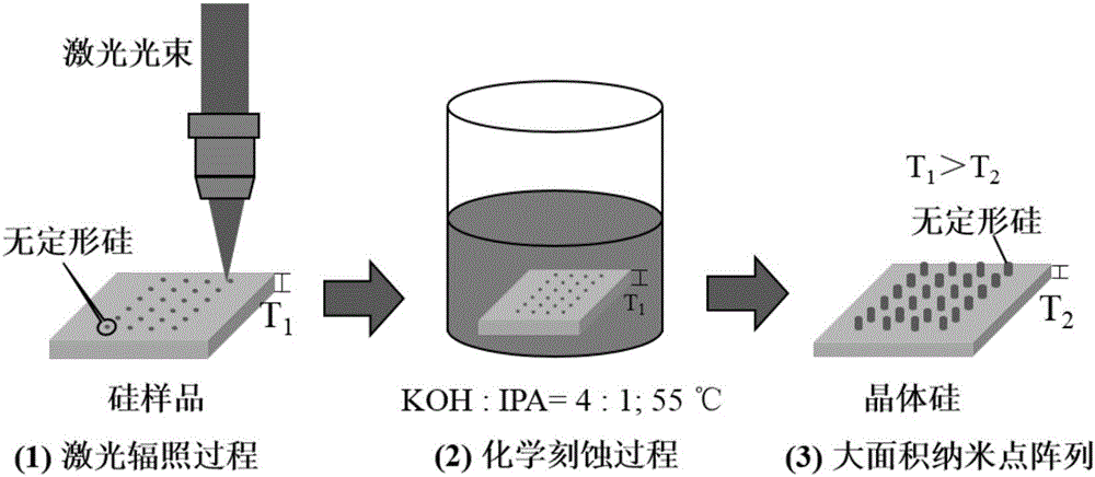
[0032] A method for efficiently processing large-area silicon micro-nano structures combined with chemical etching-assisted femtosecond laser proposed by the present invention, the processing optical path diagram and the schematic diagram of the experimental steps are as follows figure 1 and figur...


PUM


Abstract

The invention relates to a method for efficiently and controllably processing a large-area silicon micro-nano structure. The method belongs to the technical field of femtosecond laser application. The method for efficiently and controllably processing the large-area silicon micro-nano structure provided by the invention effectively utilizes the processing characteristics of an ultrafast characteristic, an ultrastrong characteristic and an ultraprecise characteristic of femtosecond laser for efficiently and controllably processing the large-area silicon micro-nano structure within a shorter time on the basis of a chemical etching-assisted femtosecond laser processing and flight time punching method; and is concretely characterized in that a local modification area is formed on a silicon surface under the action of a single laser pulse, and the chemical activity of a laser irradiation area is declined sharply, so that a mask effect can be achieved during a follow-up chemical etching process, and the processing of the maskless high-efficient and high-quality silicon micro-nano structure is further realized. Compared with the prior art, according to the method provided by the invention, a step of plating a mask layer on the surface of a processing material is omitted, so that the cost is reduced, meanwhile, the processing efficiency is improved, the method is further convenient to operate and control, and precise and controllable processing of the large-area silicon micro-nano structures under different morphologies and sizes is realized; and the processing speed is only limited by laser pulse repetition frequency.

Description

technical field [0001] The invention relates to a method for efficient and controllable processing of large-area silicon micro-nano structures, in particular to a method for efficiently and controllably processing large-area silicon micro-nano structures combined with chemical etching-assisted femtosecond lasers, belonging to the technical field of femtosecond laser applications . Background technique [0002] Silicon crystal material is currently a more important semiconductor material, mainly due to its high refractive index and its ability to be effectively integrated into complex microelectronic devices. Silicon surface micro-nanostructures with controllable morphology and arrangement have extremely important applications in the fields of microelectronics, photonics, photovoltaics, microfluidics, wetting properties, solar cells, and sensors. Silicon surface micro-nanostructures with different morphologies can be obtained by different processing methods, such as photolit...

Claims


Application Information

Patent Timeline
IPC IPC(8): B23K26/53B23K26/03B23K26/0622B23K26/062B23K26/064B81C1/00B23K101/40
CPCB23K26/032B23K26/0622B23K26/0626B23K26/064B23K26/53B23K2101/40B81C1/00214B81C1/00404B81C1/00539
Inventor 姜澜谢乾李晓炜
Owner BEIJING INSTITUTE OF TECHNOLOGYGY
Why Eureka
Try Eureka