Method for preparing display panel and prepared display panel
A display panel and substrate technology, applied in optics, instruments, nonlinear optics, etc., can solve problems such as slow response speed, achieve high aperture ratio, improve viewing angle, and simple and efficient manufacturing process and process
- Summary
- Abstract
- Description
- Claims
- Application Information
AI Technical Summary
Problems solved by technology
Method used
Image
Examples
Embodiment 1
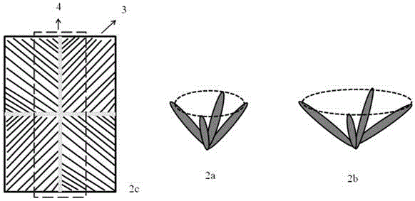
[0024] The method for preparing a multi-domain display panel includes the following steps:
[0025] S1. Coating a layer of polyimide (PI) film 1 on the first substrate (array substrate) covered by ITO on the top layer, and at the same time, coating a layer on the second substrate (color filter substrate) covered by ITO on the top layer Polyimide (PI) film 1; then pre-baked at 80°C for 3min;
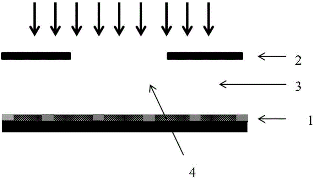
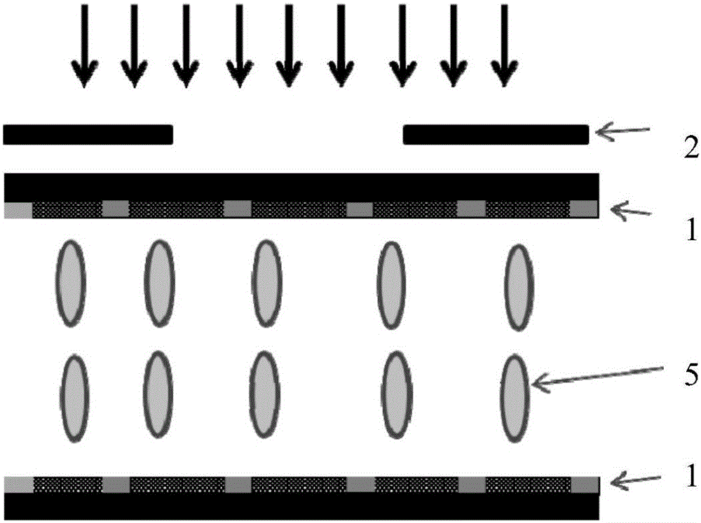
[0026] S2. Utilize patterned mask 2 to block, divide into irradiation area 4 and shielding area 3; use low-illuminance UV light (4-10mw / cm 2 ) to irradiate PI film 1, the ultraviolet light intensity is , and the irradiation time is about 5 minutes; in the irradiation area 4 (the part not covered by the mask 2), the polyimide will decompose under the irradiation of ultraviolet light, thereby reducing the alignment of the irradiation area 4 The surface anchoring energy of the membrane;
[0027] S3. Heat the alignment film on the irradiated first substrate and the second substrate to cure ...
PUM
 Abstract
Description
Claims
Application Information


