
Multiple graphical mask preparation method

A multi-patterning and masking technology, applied in semiconductor/solid-state device manufacturing, electrical components, circuits, etc., can solve problems such as sidewall differences on both sides of the sidewall, reduce shape differences, and optimize the etching process Effect

Active Publication Date: 2017-05-31
SHANGHAI HUALI MICROELECTRONICS CORP
View PDF3 Cites 3 Cited by
  • Summary
  • Abstract
  • Description
  • Claims
  • Application Information

AI Technical Summary

Problems solved by technology

[0005] The purpose of the present invention is to provide a method for preparing a multi-patterned mask, to solve the technical problem of differences in the sidewalls on both sides of the sidewall in the prior art

Method used


Image

  • Multiple graphical mask preparation method
  • Multiple graphical mask preparation method
  • Multiple graphical mask preparation method

Examples


Embodiment Construction

[0036] The preparation method of the multi-patterned mask process of the present invention will be described in more detail below in conjunction with the schematic diagram, wherein a preferred embodiment of the present invention is represented, it should be understood that those skilled in the art can modify the present invention described here, and still realize Advantageous effects of the present invention. Therefore, the following description should be understood as the broad knowledge of those skilled in the art, but not as a limitation of the present invention.

[0037] In the interest of clarity, not all features of an actual implementation are described. In the following description, well-known functions and constructions are not described in detail since they would obscure the invention with unnecessary detail. It should be appreciated that in the development of any actual embodiment, numerous implementation details must be worked out to achieve the developer's specif...


PUM

PropertyMeasurementUnit
thicknessaaaaaaaaaa
thicknessaaaaaaaaaa
thicknessaaaaaaaaaa

Abstract

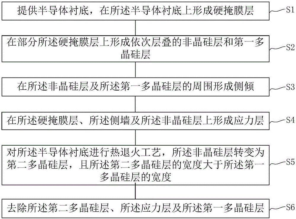
The present invention relates to a multiple graphical mask preparation method. The method comprises: providing a semiconductor substrate, and forming a hard mask layer on the semiconductor substrate; forming an amorphous silicon layer and a first polycrystalline silicon layer which are overlapped in order on part of the hard mask layer; forming a side lurch around the amorphous silicon layer and the first polycrystalline silicon layer; forming stress layers on the hard mask layer, the side wall and the amorphous silicon layer; performing heat annealing process of the semiconductor substrate, converting the amorphous silicon layer to a second polycrystalline silicon layer, wherein the width of the second polycrystalline silicon layer is larger than the width of the first polycrystalline silicon layer; and removing the second polycrystalline silicon layer, the stress layers and the first polycrystalline silicon layer. In the invention, the multiple graphical mask preparation method can reduce the morphology difference of the two side walls of the side wall so as to optimize the etching technology of the hard mark layer.

Description

technical field [0001] The invention relates to the technical field of semiconductor integrated circuit manufacturing, in particular to a method for preparing a multi-patterned mask. Background technique [0002] Semiconductor technology continues to move towards smaller process nodes driven by Moore's Law. With the continuous advancement of semiconductor technology, the functions of devices are becoming more and more powerful, but the difficulty of semiconductor manufacturing is also increasing day by day. The lithography technology is the most critical production technology in the semiconductor manufacturing process. As the semiconductor process node enters 65 nanometers, 45 nanometers, and even lower 32 nanometers, the existing 193nm ArF light source lithography technology can no longer meet the needs of semiconductor manufacturing. Extreme ultraviolet lithography (EUV), multi-beam maskless technology and nanoimprint technology have become the research hotspots of next-g...

Claims


Application Information

Patent Timeline
Patent Type & Authority Applications(China)
IPC IPC(8): H01L21/033
CPCH01L21/0337H01L21/0338
Inventor 鲍宇周海锋
Owner SHANGHAI HUALI MICROELECTRONICS CORP
Learn More