Method for verifying center deviation position of dynamic wafer in AWC (Active Wafer Centering) system

A technology for verifying dynamics and wafers, applied in semiconductor/solid-state device manufacturing, electrical components, circuits, etc., can solve problems such as not including wafers, difficult coordination of mutual positional relationship between manipulators, increased verification complexity, etc., to achieve the goal of improving efficiency Effect

Active Publication Date: 2017-05-31
SHENYANG SIASUN ROBOT & AUTOMATION
View PDF7 Cites 9 Cited by
  • Summary
  • Abstract
  • Description
  • Claims
  • Application Information

AI Technical Summary

Problems solved by technology

[0005] And because if the wafer is moved artificially, it will inevitably bring about the rotation of the wafer itself. In this case, the Δx and Δy calculated by the external equipment will include the deviation of the rotation of the wafer itself, and the result given by AWC does not include The deviation of the wafer's own rotation
If

Method used


Image

  • Method for verifying center deviation position of dynamic wafer in AWC (Active Wafer Centering) system
  • Method for verifying center deviation position of dynamic wafer in AWC (Active Wafer Centering) system
  • Method for verifying center deviation position of dynamic wafer in AWC (Active Wafer Centering) system

Examples


Embodiment Construction

[0027] The present invention will be further elaborated below in conjunction with the accompanying drawings and embodiments.

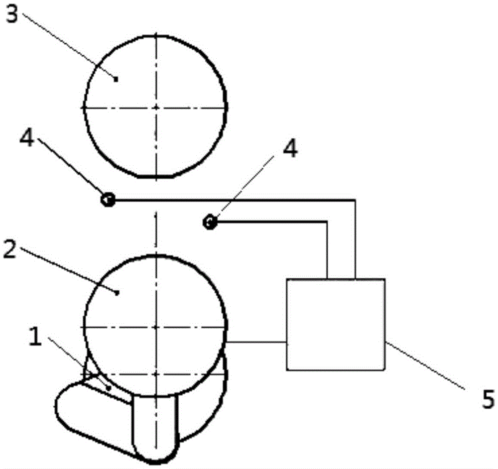
[0028] Such as figure 1 As shown, the AWC system in the prior art generally includes a manipulator 1 , a wafer 2 , a station 3 , a sensor 4 , and a manipulator controller 5 .

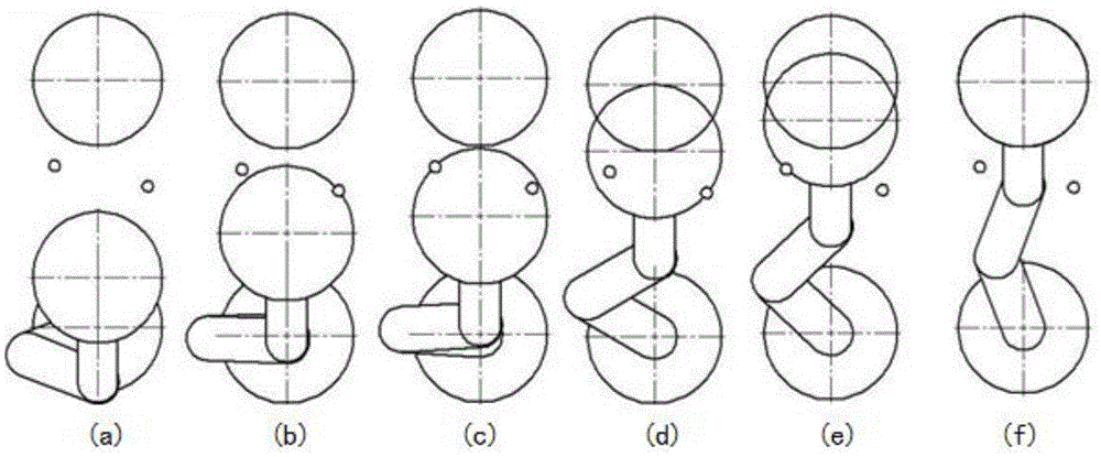
[0029] Such as figure 2 As shown, the relationship between the wafer transfer process and the sensor position in the prior art: in the taught direction, when the manipulator extends from a to f, it is a collection process; when the manipulator retracts from f to a, it is another collection process One collection process. Repeated several times, through a specific algorithm, the manipulator controller completes the zero reference calibration and stores it. After that, each time the manipulator carries the wafer in the same teaching direction (when the wafer is offset relative to the manipulator) and passes the through-beam sensor, AWC will give the deviation result of the waf...


PUM

PropertyMeasurementUnit
Outer diameteraaaaaaaaaa

Abstract

The invention relates to the technical field of mechanical control, and particularly relates to a method for verifying a center deviation position of a dynamic wafer in an AWC (Active Wafer Centering) system. The method comprises the following steps that: (1) a manipulator moves to a demonstration position above a station, an initial target sphere position is recorded by utilizing a laser tracker, and simultaneously, a current joint value on a demonstration box is recorded; (2) the manipulator drives the wafer to carry out translation, and a joint value on the demonstration box after translation is recorded; (3) the manipulator retracts and lifts the wafer to the demonstration position above the station again, and a new target sphere position is recorded; (4) an offset of a wafer center is detected by utilizing an AWC function; (5) a coordinate system is set up; and (6) according to the coordinate system, wafer deviation results obtained by display of the demonstration box, AWC detection and actual measurement of the laser tracker are respectively calculated and are compared. According to the method disclosed by the invention, the problem of translation of the wafer in the verification test is solved, no instrument or equipment is additionally added to operate the wafer, and verification test efficiency is improved.

Description

technical field [0001] The invention relates to the technical field of mechanical control, in particular to a method for verifying the center deviation position of a dynamic wafer in an AWC system. Background technique [0002] In the manufacturing process of semiconductors, manipulators are usually used between chambers or between stations to complete wafers (wafers refer to silicon wafers used in the production of silicon semiconductor integrated circuits. Because of their circular shape, they are called wafers. round) transmission. In the wafer transfer system, in order to avoid the occurrence of objective factors such as deviation or wafer damage during pick-and-place and improve the accuracy of wafer pick-and-place, it is necessary to design and use the AWC (Active Wafer Centering) system for detection and correction. The AWC system automatically corrects the deviation between the actual center and the teaching center during the movement of the manipulator to ensure th...

Claims


Application Information

Patent Timeline
IPC IPC(8): H01L21/68
CPCH01L21/68H01L21/681
Inventor 花鹏徐方邹风山张锋褚明杰张鹏
Owner SHENYANG SIASUN ROBOT & AUTOMATION
Why Eureka
Try Eureka