LED device, LED lamp and method for processing conductive bonding wire of LED device

A technology of LED devices and LED chips, which is applied in the direction of electric solid devices, semiconductor devices, circuits, etc., can solve the problems of reducing the service life of LED devices, damage to conductive bonding wires, and lack of buffering, so as to eliminate stress impact and enhance firmness performance, reduce the effect of stress shock

Active Publication Date: 2017-05-31
FOSHAN NATIONSTAR OPTOELECTRONICS CO LTD
View PDF5 Cites 9 Cited by
  • Summary
  • Abstract
  • Description
  • Claims
  • Application Information

AI Technical Summary

Problems solved by technology

[0005] However, the gold wire (conductive bonding wire) in the above-mentioned published patent is a two-dimensional structure, and its straight line section only has a certain stress buffering effect on the length direction of the gold wire (conductive bonding wire), and because the gold wire (conductive bonding wire) is The whole body is wrapped by encapsulation colloid, and the thermal expansion and contraction of the encapsulation colloid will produce stress impact on the entire conductive bonding wire, and the stress impact has no fixed direction, that is, the gold wire (conductive bonding wire) will be affected by pressure from up, down, left, right or other different directions. Stress impacts in regular directions, if these stresses are not buffered, or are only partially buffered, other conductive bonding wires that cannot be buffered by stress will be damaged in advance, thus greatly reducing the overall service life of LED devices

Method used


Image

  • LED device, LED lamp and method for processing conductive bonding wire of LED device
  • LED device, LED lamp and method for processing conductive bonding wire of LED device
  • LED device, LED lamp and method for processing conductive bonding wire of LED device

Examples


Embodiment 1

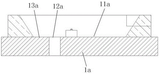
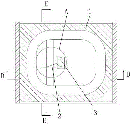
[0051] See attached figure 2 To attach Figure 8 , the invention discloses an LED device, comprising an LED chip 3, a bracket 1 for carrying the LED chip 3, a conductive bonding wire 2 connecting the LED chip electrode 30 and the bracket 1, and covering the LED chip 3 and the conductive bonding wire 2. The encapsulant of the line 2, the encapsulant is preferably silicone resin, silicone or epoxy resin, the support 1 includes an insulating area 12 and the first electrical connection area 11 and the second electrical connection area 11 located on both sides of the insulating area 12, respectively. In the connection area 13 , the LED chip 3 is mounted on the first electrical connection area 11 , one end of the conductive bonding wire 2 is located at the LED chip electrode 30 , and the other end is located at the second electrical connection area 13 .

[0052] Wherein, the LED chip 3 is a blue chip, a red chip or a green chip, which can be selected according to requirements. Whe...

Embodiment 2

[0077] Correspondingly, the present invention also discloses an LED lamp, which includes the LED device described in Embodiment 1 of the present invention, and the lamp using the LED device described in the present invention has a long service life.

Embodiment 3

[0079] Correspondingly, the present invention also discloses a method for processing the conductive bonding wire 2 of the LED device described in Embodiment 1, which includes the following steps:

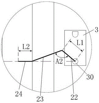
[0080] (1) After the gold ball is soldered to the LED chip electrode 30, the welding head moves upward, and the wire clip is released to form the vertical section 21;

[0081] (2) The welding head moves in the direction of the insulating area 12 according to the set track to form the first bending section 22, and can further move obliquely upward;

[0082] (3) The welding head is arranged in the direction of the second electrical connection area 13 according to the set track to form the second bending section 23. Further, it can be arranged obliquely downward in the direction of the second electrical connection area. The second bending section 23 is located in the space between the second electrical connection area 13 and the first bending section 22;

[0083] (4) Horizontally move...


PUM


Abstract

The invention discloses an LED device. The LED device comprises an LED chip, a support for bearing the LED chip, a conductive bonding wire for connecting an LED chip electrode and the support as well as a packaging glue body for covering the LED chip and the conductive bonding wire, wherein the support comprises an insulation area as well as a first electric connection area and a second electric connection area which are located on two sides of the insulation area respectively, the LED chip is mounted in the first electric connection area, one end of the conductive bonding wire is located at the LED chip electrode, the other end of the conductive bonding wire is located in the second electric connection area, and the conductive bonding wire comprises a vertical section, a first bending section, a second bending section and a connecting section. The invention further discloses an LED lamp and a method for processing the conductive bonding wire of the LED device. The stress bearing capacity of the conductive bonding wire is improved by a three-dimensional structure formed by the vertical section, the first bending section, the second bending section and the connecting section of the conductive bonding wire, so that the overall service life of the device is prolonged.

Description

technical field [0001] The invention relates to the technical field of LED devices, in particular to an LED device, an LED lamp using the LED device and a method for processing conductive welding wires in the LED device. Background technique [0002] See attached figure 1 As shown, the LED device in the prior art includes a support 1a, and the support 1a is provided with a first electrical connection area 11a, an insulating area 12a and a second electrical connection area 13a in sequence, wherein the LED chip is mounted on the first electrical connection area 11a, Among them, the LED chip and the bracket need to be connected by conductive bonding wires, so as to realize the conduction of the LED chip. After the two ends of the conductive bonding wires are respectively welded, the bracket 1a needs to be covered with encapsulating gel, and the encapsulating gel covers the LED chip and the conductive bonding wires on it. Inside. [0003] However, when using LED devices, the e...

Claims


Application Information

Patent Timeline
Patent Type & Authority Applications(China)
IPC IPC(8): H01L33/48H01L33/62
CPCH01L33/486H01L33/62H01L2224/4809H01L2224/48247H01L2224/48465H01L2924/00
Inventor 周鹏李自成霍达勋谢志国潘利兵杨璐
Owner FOSHAN NATIONSTAR OPTOELECTRONICS CO LTD
Why Eureka
Try Eureka