

Production technique of half-hole PCB
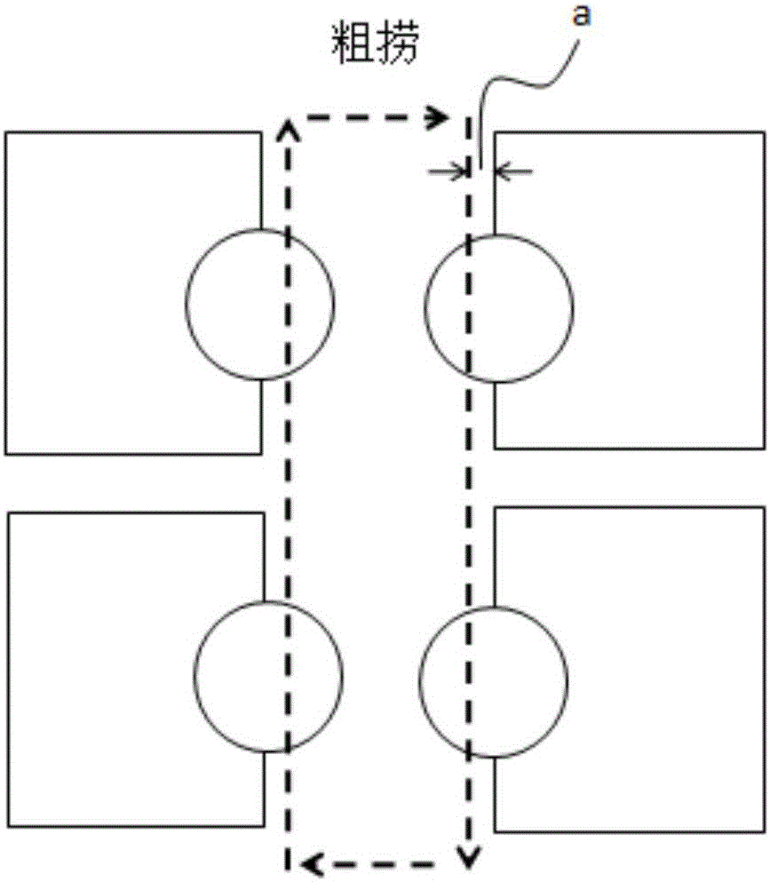
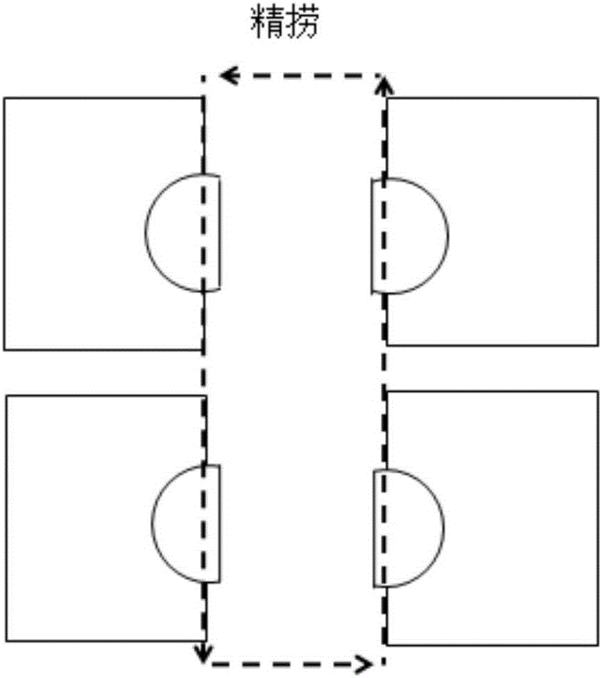
A technology of PCB board and manufacturing process, which is applied in the direction of printed circuit manufacturing, electrical connection formation of printed components, and sequence of processing steps. Avoid the pull-off effect
- Summary
- Abstract
- Description
- Claims
- Application Information
AI Technical Summary
Problems solved by technology
Method used
Image

Examples
Embodiment Construction
[0023] In order to make the above objects, features and advantages of the present invention more comprehensible, the present invention will be further described in detail below in conjunction with the accompanying drawings and specific embodiments.
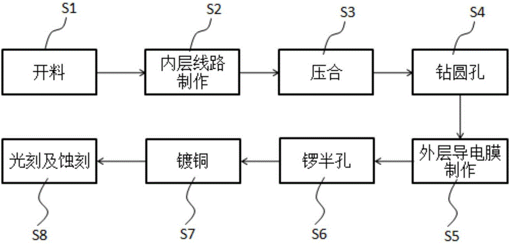
[0024] Please refer to figure 1 As shown, in a specific embodiment, the implementation steps of the manufacturing process of the half-hole PCB board provided by the invention are as follows:
[0025] S1. Material cutting: select a substrate with a thickness of 1mm and a size of 615×690mm, and the upper and lower surfaces of the material-cut substrate are covered with a copper layer with a thickness of 1 / 3OZ;
[0026] S2. Fabrication of the inner layer circuit: fabricate the inner layer circuit on the cut-out substrate to obtain a circuit board;
[0027] S3. Lamination: laminate the upper and lower sides of the circuit board with prepreg and copper foil respectively, and then perform lamination to obtain a multi-layer PCB board; ...
PUM
| Property | Measurement | Unit |
|---|---|---|
| Thickness | aaaaa | aaaaa |
| Aperture | aaaaa | aaaaa |
Abstract
Description
Claims
Application Information