Method and system for adjacent layer signal inspection of circuit board

A technology of adjacent layers and circuit boards, applied in the field of signal inspection of adjacent layers of circuit boards, can solve the problems of increasing the company's production costs, production difficulties, no inspection and prevention methods, etc.

Active Publication Date: 2017-06-09
INVENTEC PUDONG TECH CORPOARTION +1
View PDF6 Cites 0 Cited by
  • Summary
  • Abstract
  • Description
  • Claims
  • Application Information

AI Technical Summary

Problems solved by technology

[0003] The circuit board layout design software can currently provide the setting of the safety distance between different signals of the same layer for the signal layout design. The function of setting the safety distance between signals is mainly to provide the minimum distance between signals that can be produced by the circuit board factory when making circuit boards. On the other hand, it can also be used as a safe distance setting to avoid signal interference between different signals of the same layer. However, in addition to the signal interference problem of the same layer, the signals between the upper and lower adjacent layers may also cause signal interference. However, because the current layout software does not have a way to check and prevent signal interference between the upper and lower adjacent layers, engineers need to visually check one by one in the operation, and it is easy to extend these production problems due to human error, resulting in difficulties in production and further increase company production cost

Method used


Image

  • Method and system for adjacent layer signal inspection of circuit board
  • Method and system for adjacent layer signal inspection of circuit board
  • Method and system for adjacent layer signal inspection of circuit board

Examples


Embodiment Construction

[0036] In order to make the description of the present disclosure more detailed and complete, reference may be made to the accompanying drawings and various embodiments described below. However, the provided examples are not intended to limit the scope of the present invention; the description of the steps is not intended to limit the order in which they are executed, and any device that has the same effect produced by recombination is covered by the present invention scope.

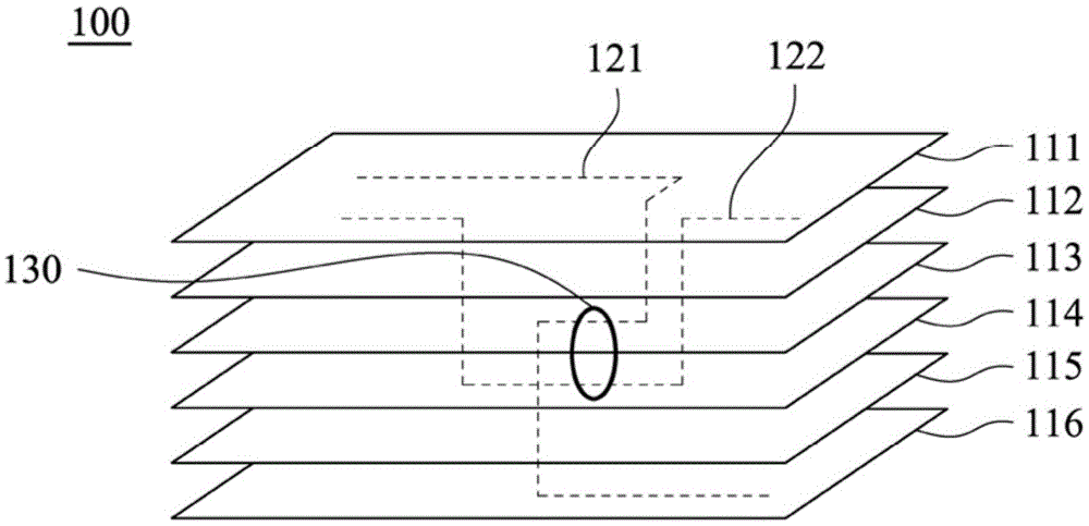
[0037] Please refer to figure 1 , figure 1 A schematic diagram of signal interference 130 in the circuit board 100 is shown. Such as figure 1 As shown, the circuit board 100 includes a plurality of layers 111-116. Although signals 121 and 122 of adjacent layers are located in different layers, when some faster signals meet certain conditions, even if they are located in different layers Cause signal interference 130. In this case, an automated system and method will be developed for this part of the...


PUM


Abstract

The invention discloses a method and system for adjacent layer signal inspection of a circuit board. The method includes acquiring an inspection range of at least one inspection signal line segment; judging whether other signal line segments of an adjacent layer exist in the inspection range; when detecting other signal line segments of the adjacent layer, combining the inspection range with the other signal line segment so as to obtain a residual area of the inspection range after the combination; deducting the residual area of the inspection range from a total area of the inspection range so as to obtain the segment area in the inspection range; dividing the segment area with a default segment width so as to obtain a segment length in the inspection range; and judging whether the segment length in the inspection range meets a default length standard or not.

Description

technical field [0001] The invention relates to a circuit board inspection technology, in particular to a method and system for inspecting signals of adjacent layers of a circuit board. Background technique [0002] The circuit board is an important electronic component, a support for electronic components, and a carrier for circuit connections of electronic components. [0003] The circuit board layout design software can currently provide the setting of the safety distance between different signals of the same layer for the signal layout design. The function of setting the safety distance between signals is mainly to provide the minimum distance between signals that can be produced by the circuit board factory when making circuit boards. On the other hand, it can also be used as a safe distance setting to avoid signal interference between different signals of the same layer. However, in addition to the signal interference problem of the same layer, the signals between the ...

Claims


Application Information

Patent Timeline
Patent Type & Authority Applications(China)
IPC IPC(8): G01R31/28
CPCG01R31/2805G06F2119/10G06F30/398
Inventor 郑永健林明慧
Owner INVENTEC PUDONG TECH CORPOARTION
Why Eureka
Try Eureka