Semiconductor embedded mixed packaging structure, and manufacturing method of the same

A technology of hybrid packaging and packaging structure, which is applied in semiconductor/solid-state device manufacturing, semiconductor devices, semiconductor/solid-state device components, etc., can solve the problems that hinder the development of miniaturization of semiconductor packaging device assembly, complex solder reflow process control, and occupation of circuit boards. Surface area and other issues, to achieve the effect of reducing the assembly area, releasing the surface area, and reducing circulation and transfer

Active Publication Date: 2017-06-09
浙江熔城半导体有限公司
View PDF3 Cites 4 Cited by
  • Summary
  • Abstract
  • Description
  • Claims
  • Application Information

AI Technical Summary

Problems solved by technology

In addition, on the surface mount, the semiconductor chip package and the circuit board are usually electrically interconnected through a solder connection. At present, the solder connection of the surface mount requires a large pad and a pad pitch of the semiconductor package device, such as a solder joint. Pad/pad spacing = 280 microns/400 microns, the precision needs to be improved, and

Method used


Image

  • Semiconductor embedded mixed packaging structure, and manufacturing method of the same
  • Semiconductor embedded mixed packaging structure, and manufacturing method of the same
  • Semiconductor embedded mixed packaging structure, and manufacturing method of the same

Examples


Embodiment Construction

[0078] The preferred embodiments of the present invention will be described in detail below in conjunction with the accompanying drawings, so that the advantages and features of the present invention can be more easily understood by those skilled in the art, so as to define the protection scope of the present invention more clearly.

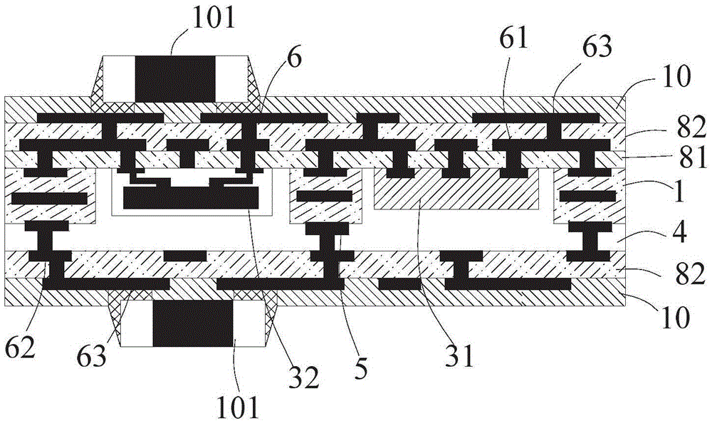
[0079] Semiconductor embedded hybrid package structure in a specific embodiment of the present invention, refer to figure 1 As shown, the package structure specifically includes:

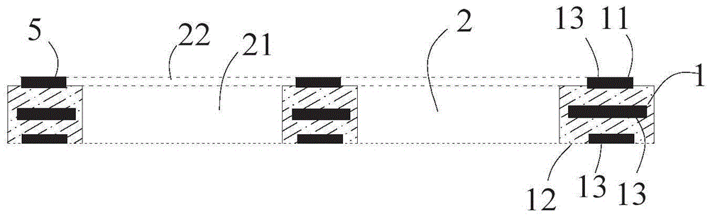
[0080] Circuit board 1, that is, a circuit carrier for packaging semiconductor chips (Bare Die) and semiconductor chip packages (Semiconductor Package), which has a first surface 11 and a second surface 12 arranged oppositely;

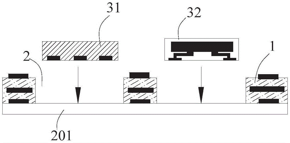
[0081] At least one opening or cavity 2 for accommodating the semiconductor chip 31 and at least one semiconductor chip package 32 provided in the circuit board 1;

[0082] A semiconductor chip 31 and a semiconductor chip package 32 disposed i...


PUM


Abstract

The invention discloses a semiconductor embedded mixed packaging structure, and a manufacturing method of the same. The embedded mixed packaging structure includes a circuit board, an opening or cavity, a semiconductor chip, a semiconductor chip package, packaging materials, and a rewiring layer, wherein the circuit board is provided with a first surface and a second surface which are arranged oppositely; the opening or cavity is arranged in the circuit board and is at least used for accommodating the semiconductor chip (Bare Die) and the semiconductor chip package (Semiconductor Package); the semiconductor chip is arranged in the opening or cavity; the semiconductor chip package is arranged in the opening or cavity; the packaging materials are at least used for covering the first surface of the circuit board and filling the space, unoccupied by the semiconductor chip and the semiconductor chip package, in the opening or cavity; and the rewiring layer is at least used for electrically connecting the semiconductor chip, the semiconductor chip package and the circuit board. The semiconductor embedded mixed packaging structure, and the manufacturing method of the same utilize the circuit board embedded technical scheme, and can simplify the integration technological process of the semiconductor chip and the semiconductor chip package, can improve the integration quality and performance, and can effectively reduce the integration area.

Description

technical field [0001] The invention relates to a circuit carrier packaging structure, in particular to a semiconductor embedded hybrid packaging structure and a manufacturing method thereof. Background technique [0002] In the prior art, the packaging of the semiconductor chip and the assembly of the semiconductor chip package are completed by the electronic packaging factory and the electronic assembly factory respectively. Firstly, the packaging of the semiconductor chip is completed, and then the semiconductor chip package is assembled on the circuit board. The assembly of the semiconductor chip package on the circuit board is usually completed by a surface mount process. [0003] Surface mount technology (Surface Mount Technology, SMT) is a method of mounting non-pin or short-lead surface mount components (SMC / SMD for short, Chinese chip components) on printed circuit boards (Printed Circuit Board, PCB) The circuit assembly technology that solders and assembles the su...

Claims


Application Information

Patent Timeline
IPC IPC(8): H01L23/31H01L23/49H01L23/528H01L21/56
CPCH01L23/528H01L21/56H01L23/3114H01L23/488H01L2224/04105H01L2224/96H01L24/96H01L24/19H01L2924/19105
Inventor 蔡亲佳
Owner 浙江熔城半导体有限公司
Why Eureka
Try Eureka