A switch device for lithium battery protection and manufacturing method thereof

A technology for switching devices and manufacturing methods, applied in semiconductor/solid-state device manufacturing, electrical components, semiconductor devices, etc., can solve the problems of large area, large internal resistance in the drift region of MOSFET, etc., and achieve regional resistance reduction and conduction internal resistance The effect of low and simple overall structure of the device

Active Publication Date: 2020-04-03
中微半导体(深圳)股份有限公司
View PDF5 Cites 0 Cited by
  • Summary
  • Abstract
  • Description
  • Claims
  • Application Information

AI Technical Summary

Problems solved by technology

[0014] In view of the above-mentioned shortcomings of the prior art, the object of the present invention is to provide a switching device for lithium battery protection and its manufacturing method, which is used to solve the large internal resistance of the drift region and the area of ​​the MOSFET for lithium battery protection in the prior art. bigger problem

Method used


Image

  • A switch device for lithium battery protection and manufacturing method thereof
  • A switch device for lithium battery protection and manufacturing method thereof
  • A switch device for lithium battery protection and manufacturing method thereof

Examples


Embodiment 1

[0060] Such as Figure 2 to Figure 9 As shown, this embodiment provides a manufacturing method for a switching device for lithium battery protection, the manufacturing method includes steps:

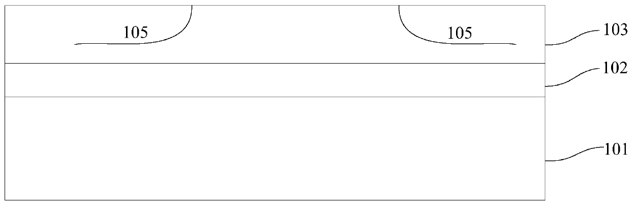
[0061] Such as figure 2 As shown, step 1) is performed first, providing a P+ type substrate 101, and forming a P− type epitaxial layer 102 on the surface of the P+ type substrate 101.

[0062] Specifically, the doping concentration of the P+ type substrate 101 is 1e18-1e19 / cm 3 , using an epitaxial method to form a P-type epitaxial layer 102 on the surface of the P+ type substrate 101, and the doping concentration of the P-type epitaxial layer 102 is 1e16-1e17 / cm 3 .

[0063] Such as figure 2 As shown, then step 2) is performed to form an N-type well region 103 in the P-type epitaxial layer 102 .

[0064] Specifically, an N-type well region 103 is formed in the P-type epitaxial layer 102 by ion implantation without a mask, and the doping concentration of the N-type well region 103...

Embodiment 2

[0088] Such as Figure 13 As shown, this embodiment provides a method for manufacturing a switching device for lithium battery protection, the basic steps of which are as in Embodiment 1, wherein the difference from Embodiment 1 is that step 2) of this embodiment includes:

[0089] Step 2-1), making a mask on the P-type epitaxial layer 102;

[0090] In step 2-2), an N-type well region 103 is formed in the P-type epitaxial layer 102 by ion implantation based on a mask, so that the gap between the N-type well region 103 and the subsequently prepared metal silicide 131 is covered. The P-type epitaxial layer 102 is isolated.

[0091] Such as Figure 13 As shown, this embodiment also provides a switching device for lithium battery protection, the basic structure of which is the same as that of Embodiment 1, wherein the difference from Embodiment 1 lies in that: the N-type well region 103 and the metal silicide The objects 131 are isolated by the P-type epitaxial layer 102 .

[...

Embodiment 3

[0094] Such as Figure 14 As shown, this embodiment provides a method for manufacturing a switching device for lithium battery protection, the basic steps of which are as in Embodiment 1, where the difference from Embodiment 1 lies in:

[0095] Step 1) also includes the step of forming an STI isolation region 121 in the P-type epitaxial layer 102, the STI isolation region 121 is located between the two gate structures 104 fabricated subsequently, and the N-type drift region prepared subsequently Region 106 surrounds the STI isolation region 121 . as well as

[0096] Step 2) includes:

[0097] Step 2-1), making a mask on the P-type epitaxial layer 102;

[0098] In step 2-2), an N-type well region 103 is formed in the P-type epitaxial layer 102 by ion implantation based on a mask, so that the gap between the N-type well region 103 and the subsequently prepared metal silicide 131 is covered. The P-type epitaxial layer 102 is isolated.

[0099] Such as Figure 14 As shown, t...


PUM


Abstract

The invention provides a switch device used for lithium battery protection and a manufacturing method thereof. The switch device includes a P+ type substrate, a P- type epitaxial layer, an N type well region, two P type well regions, two gate structures, a common N- type drifting region, N type source regions, P+ type contact region, a groove, a metal silicide, a dielectric layer and an electrode material, wherein the common N- type drifting region is formed between the two gate structures, the groove is formed in the body contact region, the metal silicide is connected with the first N type source region and the P+ type substrate based on the groove, a contact window of the second N type source region is opened in the dielectric layer, and the contact window is filled with the electrode material. According to the switch device and the manufacturing method, an MOSFET device is constructed by adopting the common drifting region, the resistance of the drifting region can be largely reduced, and at the same time, voltage resistance is kept constant. The contact of one of source region is introduced to the reverse side of a chip by using the electric conduction mode of the metal silicide and can be welded to the substrate during packaging, one wire bonding resistor is omitted, the switch device is very effective when the internal resistance requirement is low, and the overall structure of the switch device is very simple.

Description

technical field [0001] The invention relates to a lithium battery protection circuit, in particular to a switching device for lithium battery protection and a manufacturing method thereof. Background technique [0002] With the advancement of science and technology and social development, portable devices such as mobile phones, notebook computers, MP3 players, PDAs, handheld game consoles, and digital cameras have become more and more popular. Many of these products are powered by lithium-ion batteries. Lithium-ion batteries It is divided into two types: primary battery and secondary battery. At present, non-rechargeable primary lithium batteries are mainly used in some portable electronic products with low power consumption, while notebook computers, mobile phones, PDAs, digital cameras, etc. consume a lot of power. Rechargeable secondary batteries, namely lithium-ion batteries, are used in electronic products. [0003] Compared with nickel-cadmium and nickel-metal hydride...

Claims


Application Information

Patent Timeline
Patent Type & Authority Patents(China)
IPC IPC(8): H01L21/8234H01L27/088H01L29/417
CPCH01L21/8234H01L21/823418H01L21/823487H01L27/088H01L29/41741
Inventor 王凡
Owner 中微半导体(深圳)股份有限公司
Why Eureka
Try Eureka