[0028] As described in the background art, the existing three-dimensional NAND flash memory cell has a complicated manufacturing process and a large volume, which will reduce the space utilization of the chip.
[0029] Combining a three-dimensional NAND flash memory storage unit, the reasons for the complicated manufacturing process and large volume of the three-dimensional NAND flash memory storage unit are analyzed.
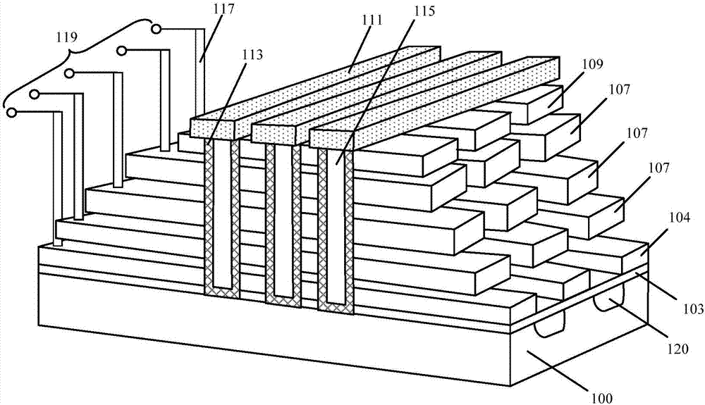
[0030] Please refer to figure 1 , figure 1 It is a schematic structural diagram of an existing three-dimensional NAND gate flash memory cell, including: a substrate 100; an isolation layer 103 on the surface of the substrate 100; a bottom selection gate 104 on the surface of the isolation layer 103; Several layers of overlapping control gates 107 on the gate 104; the top selection gate 109 located on the control gate 107; the liner between the bottom selection gate 104, the control gate 107 and the top selection gate 109 that are overlapped in two adjacent rows The source line doped region 120 in the bottom; the channel via hole (not labeled) that penetrates the top layer selection gate 109, the control gate 107, the bottom layer selection gate 104 and the isolation layer 103; located on the sidewall surface of the channel via The trench plug 113; the insulating layer 115 located on the surface of the trench plug 113 in the trench through hole, the insulating layer 115 fills the trench through hole; located in the plurality of trench plugs 113 A number of bit lines 111 on the top surface; a number of word line plugs 117 on the surface of the control gate 107 of each layer; and a number of word lines 119 on the top of the word line plugs 117.
[0031] It should be noted that the adjacent bottom-level select gate 104, control gate 107, top-level select gate 109, and bit line 111 are isolated from each other by a dielectric layer, and figure 1 To ignore the schematic diagram of the structure of the dielectric layer.
[0032] In the structure of the three-dimensional NAND gate flash memory cell, it is necessary to form one or more word line plugs 117 on the surface of each layer of the bottom select gate 104, control gate 107, or top select gate 109, and the word A number of word lines 119 need to be formed on the top surface of the line plug 117, and each word line 119 needs to be connected to a bottom layer selection gate 104, a control gate 107 or a top layer selection gate 109 through the word line plug 117, so The number of the word lines 119 is the same as the number of the bottom layer selection gate 104, the control gate 107 and the top layer selection gate 109. Since the surface of each layer of bottom select gate 104, control gate 107 and top select gate 109 needs to be formed with word line plugs 117, the number and density of word line plugs 117 that need to be formed are larger, and with the three-dimensional The size of the flash memory cell of the NAND gate is reduced, and the diameter of the word line plug 117 to be formed is smaller, which causes the difficulty of the process of forming the word line plug 117 to increase.
[0033] In order to solve the technical problem, the present invention provides a three-dimensional memory, including: a substrate, the substrate includes adjacent device regions and connection regions; a plurality of discrete devices located on the device region and the connection region substrate The stacked structure includes multiple overlapping gates; an isolation layer located on the substrate of the device area between adjacent stacked structures; a connection structure located on the substrate of the connection area, the The connection structure connects adjacent stacked structures, the connection structure includes multiple overlapping electrical connection layers, and the two ends of each electrical connection layer are respectively connected to the gates located on the same layer in the adjacent stacked structures; A number of plugs on the pole surface are electrically connected to the gate that is in contact, the gate that is on the same layer as the gate that is in contact, and the electrical connection layer that is on the same layer as the gate that is in contact.
[0034] Wherein, by connecting the gates of the same layer in the adjacent stacked structure through the electrical connection layer, the electrical connection of the gates of the same layer in the adjacent stacked structure can be realized, and the gates of the same layer in the adjacent stacked structure One plug can be shared to realize the electrical connection between the gate and the external circuit. Therefore, the forming method can reduce the number of plugs, simplify the process, reduce the volume of the memory, and improve the space utilization rate of the chip.
[0035] In order to make the above-mentioned objects, features and advantages of the present invention more obvious and understandable, specific embodiments of the present invention will be described in detail below with reference to the accompanying drawings.
[0036] Figure 2 to Figure 12 It is a schematic structural diagram of each step of a method for forming a three-dimensional memory according to an embodiment of the present invention.
[0037] Please refer to figure 2 , A substrate 200 is provided, and the substrate 200 includes adjacent device regions A and connection regions B.
[0038] The device area A and the connection area B are used to form a stacked structure; the connection area B is also used to form a connection structure connecting adjacent stacked structures.
[0039] The substrate 200 further includes a channel region C adjacent to the connection region B or the device region A.
[0040] In this embodiment, the channel region C is adjacent to the connection region B, and the connection region B is located between the device region A and the channel region C. In other embodiments, the device region may be located on both sides of the connection region, and the channel region is adjacent to the device region.
[0041] In this embodiment, the substrate 200 is a silicon substrate, a silicon germanium substrate, a silicon carbide substrate, a silicon-on-insulator substrate, a germanium-on-insulator substrate, a glass substrate, or a III-V compound substrate (for example, Gallium nitride substrate or gallium arsenide substrate, etc.).
[0042] Subsequently, a plurality of discrete stacked structures and isolation layers on the device area A substrate 200 between adjacent stacked structures are formed on the substrate 200 of the device region A and the connection region B, and the stacked structure includes multiple layers. A gate electrode with overlapping layers; a connecting structure is formed on the substrate 200 in the connection area B, the connecting structure connects adjacent stacked structures, the connecting structure includes multiple overlapping electrical connection layers, the electrical connection layer Connect the gates on the same layer in the adjacent stacked structure.
[0043] In this embodiment, the steps of forming the laminated structure, isolation layer and connection structure are as follows: Figure 3 to Figure 10 Shown.
[0044] In this embodiment, the stacked structure includes a gate structure of a transistor, and the substrate 200 on both sides of the gate structure has source and drain regions, and the source and drain regions and the substrate 200 on both sides of the gate structure are It has a shallow trench isolation structure.
[0045] Please refer to image 3 with Figure 4 , image 3 Is in figure 2 Schematic diagram based on, Figure 4 Yes image 3 Along the cross-sectional view of the cutting line 1-2, a composite layer is formed on the substrate 200 of the device area A and the connection area B, and the composite layer includes a plurality of insulating layers 212 and a plurality of sacrificial layers 211 that are overlapped alternately.
[0046] The insulating layer 212 subsequently realizes electrical isolation between adjacent gates, and the sacrificial layer 211 is used to occupy space for the gates to be formed later.
[0047] The composite layer is also located on the channel region C substrate 200.
[0048] The step of forming the composite layer includes: forming a sacrificial layer 211 on the substrate 200 of the device region A, the connecting region B and the channel region C; forming an insulating layer 212 on the sacrificial layer 211; and repeatedly forming the sacrificial layer The steps of layer 211 and insulating layer 212 form the composite layer.
[0049] In this embodiment, the material of the sacrificial layer 211 is polysilicon or silicon nitride. In other implementations, the material of the sacrificial layer may also be polycrystalline germanium or polycrystalline silicon germanium.
[0050] In this embodiment, the process of forming the sacrificial layer 211 includes a chemical vapor deposition process. In other embodiments, the process of forming the sacrificial layer may include a physical vapor deposition process.
[0051] In this embodiment, the material of the insulating layer 212 is silicon oxide.
[0052] In this embodiment, the process of forming the insulating layer 212 includes a chemical vapor deposition process. In other embodiments, the process of forming the sacrificial layer may include a physical vapor deposition process or an atomic layer deposition process.
[0053] After forming the composite layer, the forming method further includes: etching the composite layer to expose part of the surface of the sacrificial layer of each layer.
[0054] Please refer to Figure 5 with Image 6 , Figure 5 Is in image 3 Schematic diagram based on, Image 6 Yes Figure 5 Along the cross-sectional view of the cutting line 3-4, a channel plug 220 is formed on the substrate 200 in the channel region C.
[0055] The channel plug 220 is used as a channel of the formed three-dimensional memory. The channel plug and the subsequent gate are used as transistors of the three-dimensional memory.
[0056] The channel plug 220 is located in the composite layer of the channel region C.
[0057] The step of forming the channel plug 220 includes: etching the composite layer, forming a through hole in the composite layer of the channel region C, and the through hole penetrates the composite layer; A trench plug 220 is formed on the sidewall surface.
[0058] In this embodiment, the process for etching the composite layer includes a dry etching process or a wet etching process.
[0059] The step of forming the channel plug 220 in the through hole includes: forming an amorphous layer on the surface of the sidewall of the through hole; and annealing the amorphous layer to form the channel plug 220.
[0060] In this embodiment, the material of the amorphous layer is amorphous silicon. In other embodiments, the material of the amorphous layer may be amorphous silicon germanium, amorphous germanium or amorphous silicon carbide.
[0061] The process of forming the amorphous layer includes a chemical vapor deposition process.
[0062] The annealing treatment is used to crystallize the amorphous layer to form crystals.
[0063] In this embodiment, the material of the channel plug 220 is monocrystalline silicon. In other embodiments, the material of the channel plug is silicon germanium, silicon carbide or germanium.
[0064] Please refer to Figure 7 , Figure 7 Is in Figure 5 Based on the schematic diagram of the subsequent steps, the composite layer is patterned, and a part of the composite layer in the device area A is removed to form a trench 221, which penetrates the composite layer in a direction perpendicular to the surface of the substrate 200 And the extending direction of the trench 221 is perpendicular to the direction of the boundary line between the device area A and the connection area B, leaving the connection area B composite layer.
[0065] It should be noted that since the composite layer of the connection area B is retained, the sacrificial layer in the composite layer of the connection area B can provide space for the subsequent formation of the electrical connection layer, thereby enabling the gate electrode in the adjacent laminated structure The electrical connection can further reduce the number of plugs formed subsequently, reduce the volume of the memory, simplify the process, and reduce the cost.
[0066] The step of patterning includes: forming a mask layer on the composite layer, the mask layer covering the connection area B composite layer and part of the composite layer of the device area A; taking the mask layer as The mask etches the composite layer.
[0067] In the laminated structure, the insulating layer between two adjacent layers of gates is a first insulating layer, and the first insulating layer is used to achieve electrical insulation between two adjacent layers of gates; The insulating layer between two adjacent electrical connection layers is a second insulating layer, and the second insulating layer is used to realize electrical insulation between two adjacent electrical connection layers.
[0068] In this embodiment, the material of the mask layer is photoresist.
[0069] In this embodiment, the process for etching the composite layer includes a dry etching process or a wet etching process.
[0070] Please refer to Picture 8 , Picture 8 Is in Figure 7 Based on the schematic diagram of subsequent steps, an isolation layer 222 is formed in the trench 221.
[0071] The isolation layer 222 is used to achieve electrical insulation between different laminated structures.
[0072] In this embodiment, the material of the isolation layer 222 is silicon oxide. In other embodiments, the material of the isolation layer may also be silicon oxynitride.
[0073] The process of forming the isolation layer 222 includes a chemical vapor deposition process, a physical vapor deposition process, or an atomic layer deposition process.
[0074] Please refer to Picture 9 , Picture 9 Is in Image 6 Based on the schematic diagram of the subsequent steps, the sacrificial layer 211 of the device region A and the connection region B (such as Image 6 As shown), a number of grooves 230 are formed between adjacent insulating layers 212.
[0075] The groove 230 exposes the surface of the channel plug 220.
[0076] It should be noted that since the connection area A substrate 200 has a composite layer, after removing the sacrificial layer 211, the connection area A has a groove, and the groove in the connection area A is connected to the isolation Grooves on both sides of layer 222.
[0077] The process of removing the sacrificial layer 211 of the device region A and the connection region B includes isotropic dry etching or wet etching.
[0078] In this embodiment, the material of the sacrificial layer 211 is silicon nitride; when the isotropic etching process is a wet etching process, the etching solution for the wet etching includes phosphoric acid; When the isotropic etching process is a dry etching process, the dry etching process includes: the etching gas includes CF 4 , CHF 3 , C 4 F 8 , C 4 F 6 , CH 2 F 2 One or more of them, the power is less than 100 watts, and the bias voltage is less than 10 volts.
[0079] Please refer to Picture 10 , In the device area A and the connection area B a number of grooves 230 (such as Picture 9 As shown in), a gate layer 231 is formed, the gate layer 231 of the device region A and the gate layer of the connection region adjacent to the isolation layer constitute the gate, and the gate layer 231 connected to the gate of the connection region B constitutes The electrical connection layer.
[0080] It should be noted that, by connecting the same-layer gates in adjacent stacked structures through the electrical connection layer, electrical connection of the same-layer gates in adjacent stacked structures can be achieved, and the same layer in adjacent stacked structures The layer gate can share a plug to realize the electrical connection between the gate and the external circuit. Therefore, the forming method can reduce the number of plugs, simplify the process, reduce the volume of the memory, and improve the space utilization rate of the chip.
[0081] The step of forming the gate layer 231 includes: forming an initial gate layer on the sidewall and surface of the insulating layer 212 in the groove 230 of the device region A and the connecting region B; removing the side of the insulating layer 212 The initial gate layer on the wall and the surface forms a gate layer 231.
[0082] In this embodiment, the gates of each layer in the adjacent stacked structure are connected by an electrical connection layer. The connection structure includes a plurality of electrical connection layers. In other embodiments, part of the gates in adjacent stacked structures are connected by an electrical connection layer.
[0083] In this embodiment, the material of the gate layer 231 is tungsten. In other embodiments, the material of the gate layer may also be aluminum or copper.
[0084] In this embodiment, the process for forming the initial gate layer is a chemical vapor deposition process or an atomic layer deposition process.
[0085] In this embodiment, the process of removing the initial gate layer on the sidewall and surface of the insulating layer 212 includes a dry etching process.
[0086] It should be noted that, before forming the gate layer 231, it further includes: forming a gate dielectric layer on the bottom and sidewall surfaces of the groove 230.
[0087] In this embodiment, the material of the gate dielectric layer is a high-k (k less than 3.9) dielectric material. In other embodiments, the gate dielectric layer may further include: a first silicon oxide layer on the bottom and sidewall surfaces of the groove; a silicon nitride layer on the surface of the first oxide layer; The second silicon dioxide layer on the surface of the silicon layer.
[0088] Please refer to Picture 11 with Picture 12 , Picture 12 Yes Picture 11 Along the cross-sectional view of the cutting line 5-6, a number of plugs 232 are formed on the surface of each layer of the gate. Each plug 232 is in contact with the gate, the gate in the same layer as the contacted gate, and the The electrical connection layers on the same layer are electrically connected.
[0089] The plug 232 is used to realize the electrical connection between the gate and the external circuit, so as to realize the control of the transistor in the three-dimensional memory.
[0090] In this embodiment, the material of the plug 232 is tungsten. In other embodiments, the material of the plug may also be copper.
[0091] Since the electrical connection layer is connected to the gates in the adjacent stacked structure, the electrical connection of the gates in the adjacent stacked structure can be realized, and the electrically connected gates can share a plug 232, thereby realizing the gate The electrical connection between the pole and the external circuit. Therefore, the number of the plugs 232 is small, and therefore the production cost can be reduced.
[0092] To sum up, in this embodiment, the same-layer gates in adjacent stacked structures are connected through the electrical connection layer to achieve electrical connection of the same-layer gates in adjacent stacked structures. The gates of the same layer in the same layer can share a plug to realize the electrical connection between the gate and the external circuit. Therefore, the forming method can reduce the number of plugs, simplify the process, reduce the volume of the memory, and improve the space utilization rate of the chip.
[0093] Continue to refer Picture 11 with Picture 12 , An embodiment of the present invention also provides a three-dimensional memory, including: a substrate 200, the substrate 200 includes an adjacent device area A and a connection area B; located on the device area A and the connection area B substrate 200 A plurality of discrete stacked structures, the stacked structures including multiple overlapping gates; an isolation layer 222 on the substrate 200 in the device region A between adjacent stacked structures; the substrate in the connecting region B 200, the connection structure connects adjacent laminated structures, the connection structure includes multiple overlapping electrical connection layers, and the two ends of each electrical connection layer are respectively connected to the adjacent laminated structures on the same layer Gate; plugs 232 on the surface of the gate, each plug 232 and the gate in contact, the gate in the same layer as the gate in contact, and the electrical connection layer in the same layer as the gate in contact Electric connection.
[0094] The electrical connection layer is made of the same material as the gate electrode. Specifically, in this embodiment, the material of the electrical connection layer and the gate is tungsten. In other embodiments, the material of the electrical connection layer and the gate may also be aluminum or tungsten.
[0095] The laminated structure further includes: a first insulating layer located between adjacent gates; the connection structure further includes: a second insulating layer located between adjacent electrical connection layers. The first insulating layer and the second insulating layer constitute an insulating layer 222.
[0096] In this embodiment, the material of the insulating layer 222 is silicon oxide.
[0097] The substrate 200 further includes a channel region C, and the channel region C is adjacent to the connection region B or the device region A; the stacked structure also extends to the channel region C on the substrate 200.
[0098] The three-dimensional memory further includes: a plurality of channel plugs 220 on the substrate 200 in the channel region C, and the channel plugs 220 penetrate the laminated structure.
[0099] The three-dimensional memory further includes: a gate dielectric layer between the gate and the channel plug 220.
[0100] In summary, in this embodiment, a connection structure for connecting adjacent stacked structures is formed on the substrate in the connection area, and the connection structure includes an electrical connection layer that connects the gates in the adjacent stacked structures. By connecting the same-layer gates in adjacent stacked structures through the electrical connection layer, electrical connection of the same-layer gates in adjacent stacked structures can be realized, and the same-layer gates in adjacent stacked structures can be shared A plug to achieve electrical connection between the gate and the external circuit. Therefore, the forming method can reduce the number of plugs, simplify the process, reduce the volume of the memory, and improve the space utilization rate of the chip.
[0101] Although the present invention is disclosed as above, the present invention is not limited to this. Any person skilled in the art can make various changes and modifications without departing from the spirit and scope of the present invention. Therefore, the protection scope of the present invention should be subject to the scope defined by the claims.