

A light-emitting diode epitaxial growth method and light-emitting diode
A light-emitting diode and epitaxial growth technology, which is applied in semiconductor devices, electrical components, circuits, etc., can solve the problems of reduced luminous efficiency and uneven current distribution, achieve uniform current distribution, avoid uneven current distribution, and improve luminous efficiency. Effect
- Summary
- Abstract
- Description
- Claims
- Application Information
AI Technical Summary
Problems solved by technology
Method used
Image

Examples
Embodiment 1
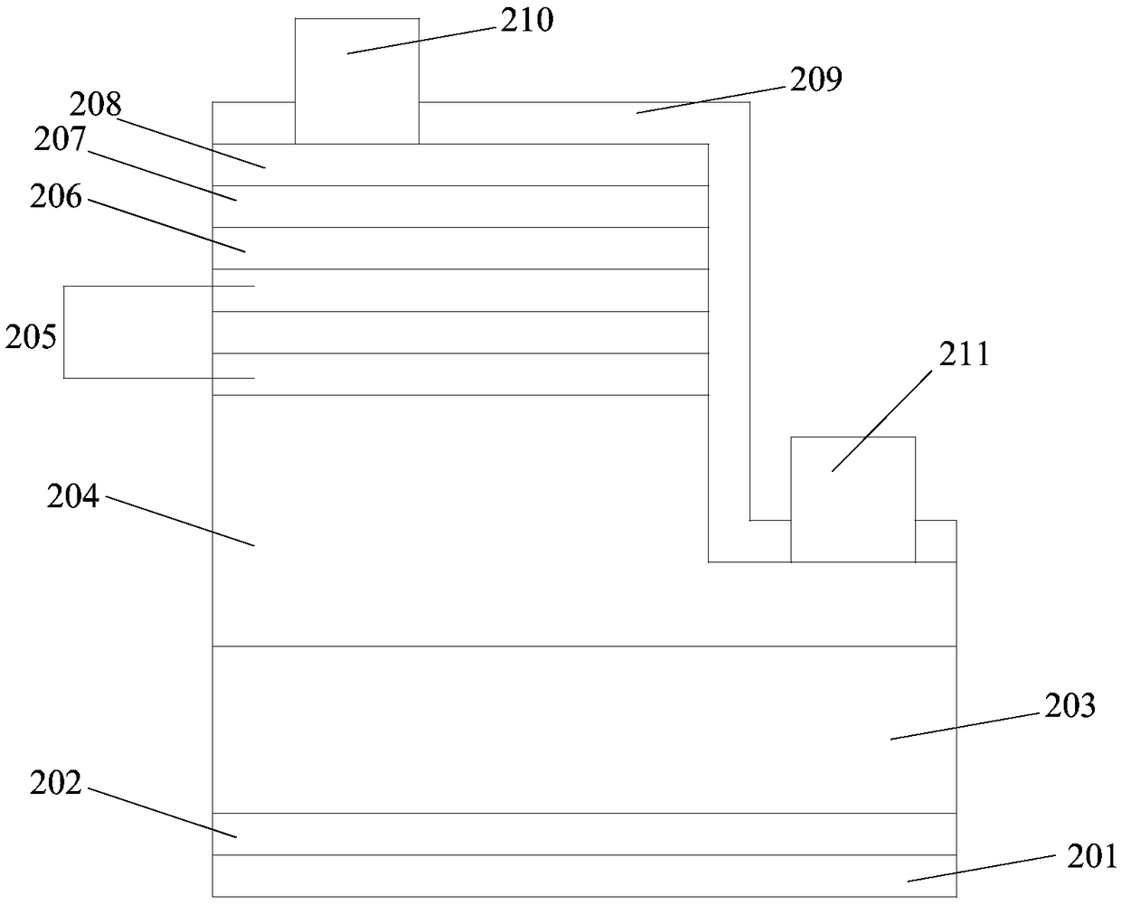
[0053] Such as figure 1 Shown is a schematic diagram of the structure of the LED prepared by the prior art method. The LED structure epitaxial growth method in the prior art includes the following steps:
[0054] Step 101, processing the sapphire substrate:
[0055] Under the hydrogen atmosphere of 1000-1100°C, feed 100L / min-130L / min of H 2 , keep the reaction chamber pressure at 100-300mbar (air pressure unit), and process the sapphire substrate for 5-10 minutes.
[0056] Step 102, growing a low-temperature buffer layer GaN:
[0057] Cool down to 500-600°C, keep the reaction chamber pressure at 300-600mbar, and feed NH with a flow rate of 10000-20000sccm (sccm remark standard ml per minute) 3 , 50-100sccm TMGa and 100L / min-130L / min H 2 , grow a low-temperature buffer layer GaN with a thickness of 20-40nm on a sapphire substrate.
[0058] Step 103, low temperature buffer layer GaN etching treatment:
[0059] Raise the temperature to 1000-1100°C, keep the reaction chambe...
Embodiment 2
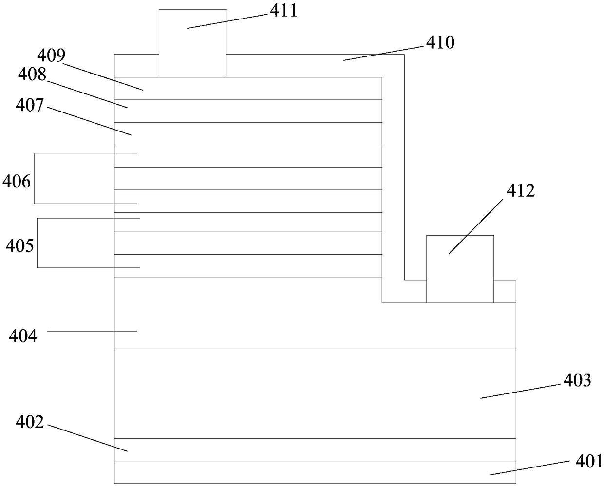
[0096] The light emitting diode epitaxial growth method described in this embodiment includes the following steps:
[0097] Step 501, processing the sapphire substrate: in a hydrogen atmosphere at 1000-1100°C, inject 100L / min-130L / min of H 2 , keeping the pressure of the reaction chamber at 100-300 mbar, and processing the sapphire substrate for 5-10 minutes.
[0098] Step 502, growing low-temperature buffer layer GaN: at a temperature of 500-600°C, a reaction chamber pressure of 300-600mbar, and a flow rate of 10000-20000sccm of NH 3 , 50-100sccm TMGa and 100L / min-130L / min H 2 Under the condition of , a low temperature buffer layer GaN with a thickness of 20-40nm is grown on the sapphire substrate.
[0099] Step 503, low-temperature buffer layer GaN etching treatment: raise the temperature to 1000-1100°C, keep the reaction chamber pressure at 300-600mbar, and feed NH at a flow rate of 30000-40000sccm 3 And 100L / min-130L / min H 2 Under the condition of keeping the temperatu...
Embodiment 3
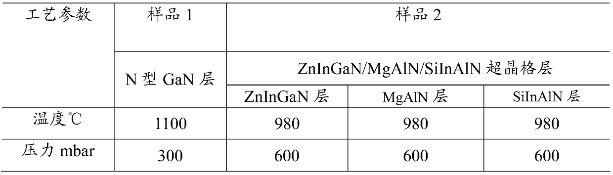
[0115] This example provides a comparison example of the luminous performance of the light-emitting diode of the present invention and the light-emitting diode of the traditional solution. The comparative method of the present embodiment comprises the following contents:
[0116] Prepare sample 1 according to the traditional LED growth method, and prepare sample 2 according to the method described in the present invention; the difference between sample 1 and sample 2 epitaxial growth method parameters is that the preparation process of sample 2 grows a ZnInGaN / MgAlN / SiInAlN superlattice layer , the other epitaxial layer growth conditions of sample 1 and sample 2 are exactly the same (please refer to Table 1). Sample 1 and sample 2 were plated with an ITO layer with a thickness of about 150nm under the same pre-process conditions, and a Cr / Pt / Au electrode with a thickness of about 1500nm was plated under the same conditions, and the plated thickness was about 1500nm under the s...
PUM
 Abstract
Description
Claims
Application Information