Shifting register unit and shifting register

A shift register and reset unit technology, applied in static memory, digital memory information, instruments, etc., can solve the problems of display image quality, large delay of output pulse voltage signal, long time of output voltage signal drop, etc.

Active Publication Date: 2017-07-04
BOE TECH GRP CO LTD
View PDF7 Cites 9 Cited by
  • Summary
  • Abstract
  • Description
  • Claims
  • Application Information

AI Technical Summary

Problems solved by technology

Each shift register unit is usually composed of multiple transistors and capacitors. Since the existing shift register unit is a DC output, the delay of the output pulse voltage signal at the output terminal is relatively long, that is, the output volta

Method used


Image

  • Shifting register unit and shifting register
  • Shifting register unit and shifting register
  • Shifting register unit and shifting register

Examples


Embodiment 1

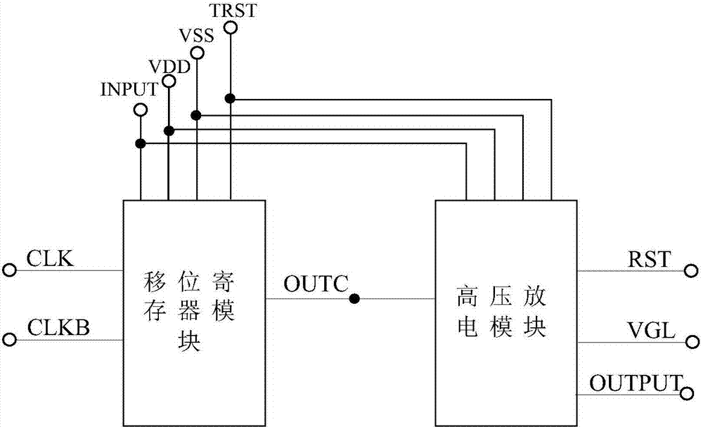
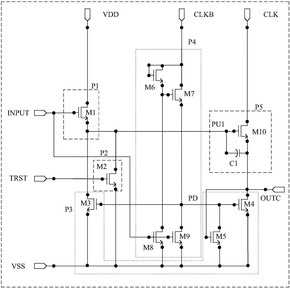
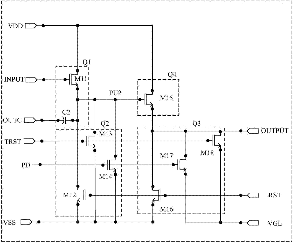
[0049] figure 1 Schematic diagram of the structure of the shift register unit provided for the embodiment of the present invention, such as figure 1 As shown, the shift register unit provided by the embodiment of the present invention includes: a shift register module and a high voltage discharge module.

[0050] Wherein, the shift register module is connected to the signal input terminal INPUT, the first reset signal terminal TRST, the first low level terminal VSS, the high level terminal VDD, the first clock signal terminal CLKB and the second clock signal terminal CLK. The high-voltage discharge module is connected to the output terminal OUTC, the high-level terminal VDD, the signal input terminal INPUT, the first reset signal terminal TRST, the second reset signal terminal RST, the first low-level terminal VSS and the second low-level terminal of the shift register module. Flat end VGL.

[0051] It should be noted that the output end of the shift register unit is the out...

Embodiment 2

[0097] Based on the technical conception of the technical solution of embodiment one, Figure 7 Schematic diagram of the structure of the shift register provided for the embodiment of the present invention, such as Figure 7 As shown, the shift register provided in Embodiment 2 of the present invention includes a plurality of shift register units.

[0098] Wherein, except the first-stage shift register unit, the signal input end of each other shift register unit is connected to the current-stage output end of the adjacent upper-stage shift register unit; except the last-stage shift register unit, The output end of each other shift register unit at this stage is connected to the reset signal end of the upper shift register unit adjacent to it.

[0099] Specifically, the input terminal INPUT2 of the second shift register unit is connected to the output terminal OUTPUT1 of the first shift register unit, and the input terminal INPUT3 of the third shift register unit is connected ...


PUM


Abstract

The invention discloses a shifting register unit and a shifting register, and the shifting register unit comprises a shifting register module and a high-voltage discharge module; wherein the shifting register module is connected with a signal input end, a first reset signal end, a first low level end, a high level end, a first clock signal end and a second clock signal end; and the high-voltage discharge module is connected with an output end, a high level end, a signal input end, a first reset signal end, a second reset signal end, a first low level end and a second low level end of the shifting register module. According to the invention, the shifting register unit comprises the high-voltage discharge module which is connected with the shifting register module in series, the voltage difference of power supply for grid line is increased, the discharge speed is improved, the time of output voltage signal decrease is reduced, and the high-resolution requirement of an existing display device is met.

Description

technical field [0001] The invention relates to the field of display technology, in particular to a shift register unit and a shift register. Background technique [0002] In recent years, flat panel displays, such as Thin Film Transistor-Liquid Crystal Display (TFT-LCD) and Active Matrix Organic Light Emitting Diode (AMOLED), have been It is widely used in electronic products such as TVs and mobile phones because of its advantages of thinness and low power consumption. [0003] A TFT-LCD or AMOLED display panel is composed of a matrix of pixels in both horizontal and vertical directions, and each pixel in the display panel is driven to display by a driving circuit. The drive circuit mainly includes a gate drive circuit and a data drive circuit, wherein the data drive circuit is used to sequentially latch the input data according to the clock signal and convert the latched data into an analog signal and input it to the data line of the display panel. The gate drive circuit...

Claims


Application Information

Patent Timeline
IPC IPC(8): G09G3/3266G09G3/36G11C19/28
CPCG09G3/3266G09G3/3674G09G2310/0286G11C19/28
Inventor 韩明夫商广良韩承佑姚星郑皓亮金志河袁丽君王志冲
Owner BOE TECH GRP CO LTD
Why Eureka
Try Eureka