Ga2O3-baesd metal oxide semiconductor field effect transistor with good heat dissipation performance and preparation method thereof

An oxide semiconductor and field effect transistor technology is applied in the field of Ga2O3-based metal oxide semiconductor field effect transistor and its preparation, and achieves the effects of easy integration, good heat dissipation and low price.

Active Publication Date: 2017-07-04
上海镓旦电子信息有限公司
View PDF5 Cites 22 Cited by
  • Summary
  • Abstract
  • Description
  • Claims
  • Application Information

AI Technical Summary

Problems solved by technology

Thus, a good heat dissipation Ga 2 o 3 Based MOSFET and its preparation me

Method used


Image

  • Ga2O3-baesd metal oxide semiconductor field effect transistor with good heat dissipation performance and preparation method thereof
  • Ga2O3-baesd metal oxide semiconductor field effect transistor with good heat dissipation performance and preparation method thereof
  • Ga2O3-baesd metal oxide semiconductor field effect transistor with good heat dissipation performance and preparation method thereof

Examples


Embodiment 1

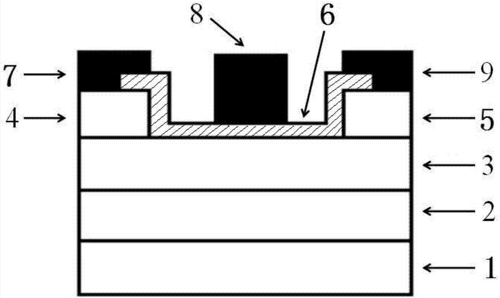
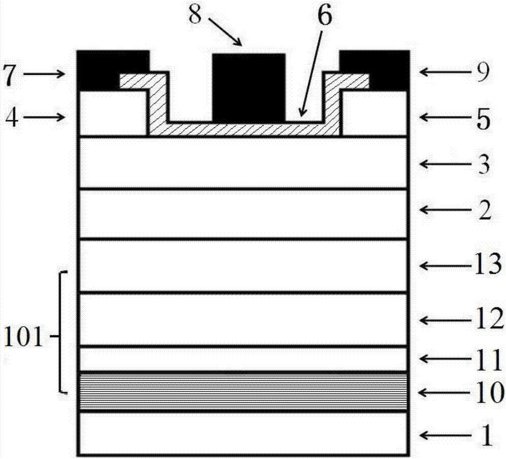
[0028] A good heat dissipation Ga 2 o 3 The base MOSFET is sequentially composed of substrate 1, Ga 2 o 3 Buffer 2, Ga 2 o 3 Epitaxial Ga on buffer layer 2 2 o 3 The channel layer 3, the mutually separated source region 4 and the drain region 5 prepared on the channel layer 3, the Al deposited on the source region 4, the drain region 5 and part of the channel layer 3 2 o 3 An insulating layer 6, a source electrode 7, a gate electrode 8 and a drain electrode 9 prepared by thermal evaporation on the source region 4, the drain region 5 and the insulating layer 6; it is characterized in that: the substrate 1 is a Si single crystal, and the substrate 1 and the Ga 2 o 3 A nitride and oxide mixed multilayer structure 101 is also prepared in the middle of the upper buffer layer 2; the mixed multilayer structure 101 is made of GaN-based multilayer structure film 10 and GaN-based multilayer structure film 10 prepared by high-temperature oxidation. 2 o 3 Thin layer 11, Ga 2 o...


PUM

PropertyMeasurementUnit
Thicknessaaaaaaaaaa
Thicknessaaaaaaaaaa
Thicknessaaaaaaaaaa

Abstract

The invention discloses a Ga2O3-baesd metal oxide semiconductor field effect transistor with good heat dissipation performance and a preparation method thereof, and belongs to the technical field of power semiconductor devices and preparation thereof. The device is formed by parts of a substrate, a Ga2O3 buffering layer, a Ga2O3 channel layer, a Ga2O3 source, a drain region, an Al2O3 insulation layer and a metal electrode, and is characterized in that the substrate is Si monocrystalline; a nitride and oxide mixed multilayer structure is prepared between the substrate and the Ga2O3 buffering layer; and the mixed multilayer structure is formed by a GaN-serial multilayer structure film, a Ga2O3 oxidation thin layer, an involuntary doped Ga2O3 lower buffering layer and a magnesium doped Ga2O3 semi-insulation layer. According to the invention, a heteroepitaxy problem of Ga2O3 materials is solved; disadvantages of poor heat dissipation performance and high selling price of the Ga2O3 monocrystalline substrate used by the current Ga2O3-baesd metal oxide semiconductor field effect transistor are overcome; and advantages of mature technology, low selling price, easy integration and good heat dissipation of the Si material can be used, so the provided Ga2O3-baesd metal oxide semiconductor field effect transistor is quite highly practical.

Description

technical field [0001] The invention belongs to the technical field of power semiconductor devices and their preparation, in particular to a class of Ga 2 o 3 A base metal oxide semiconductor field effect transistor and a manufacturing method thereof. Background technique [0002] Semiconductor power devices mainly refer to semiconductor electronic devices used in power conversion and control circuits of power equipment. Among many power devices, high-power metal-oxide-semiconductor field-effect transistor (MOSFET) devices are very important for high-voltage transmission and power conversion electrical appliances. High-voltage MOSFETs often have to withstand high voltages of hundreds or even thousands of volts, which has extremely high requirements for materials. However, the widely used Si material has a bandgap of only 1.1eV and a very small breakdown field strength, so high-voltage devices must be obtained by using bipolar devices (such as insulated gate bipolar transi...

Claims


Application Information

Patent Timeline
IPC IPC(8): H01L29/78H01L29/267H01L23/373H01L21/02
CPCH01L29/78H01L21/02381H01L21/02458H01L21/02483H01L21/02505H01L21/02565H01L21/0262H01L23/3738H01L29/267
Inventor 董鑫梁红伟张源涛夏晓川张宝林杜国同
Owner 上海镓旦电子信息有限公司
Why Eureka
Try Eureka