a high quality ga 2 o 3 Thin film and its heteroepitaxial preparation method

A heterogeneous epitaxial, high-quality technology, applied in semiconductor/solid-state device manufacturing, electrical components, circuits, etc., can solve problems such as poor quality of heterogeneous epitaxial crystals

Active Publication Date: 2021-09-10
JILIN UNIV
View PDF5 Cites 0 Cited by
  • Summary
  • Abstract
  • Description
  • Claims
  • Application Information

AI Technical Summary

Problems solved by technology

[0004] Purpose of the present invention is exactly to solve above-mentioned Ga 2 o 3 The problem of poor quality of heteroepitaxial crystals, providing a high-quality Ga 2 o 3 Thin film and its heteroepitaxial preparation method

Method used


Image

  • a high quality ga  <sub>2</sub> o  <sub>3</sub> Thin film and its heteroepitaxial preparation method
  • a high quality ga  <sub>2</sub> o  <sub>3</sub> Thin film and its heteroepitaxial preparation method

Examples


Embodiment 1

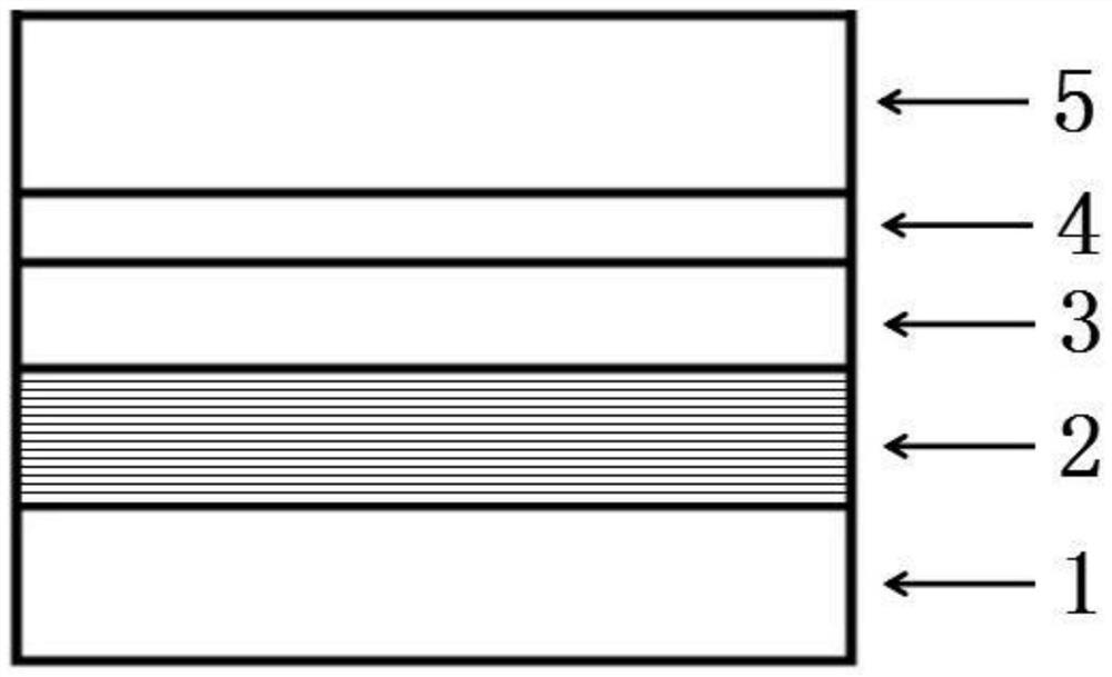
[0017] A high quality Ga 2 o 3 Heteroepitaxial thin films with structures such as figure 1 As shown, the c-plane sapphire substrate 1, the epitaxially grown GaN-based multilayer structure film 2 on the c-plane sapphire substrate 1, and the low-temperature oxidized low-temperature Ga 2 o 3 Oxide layer 3, low temperature Ga 2 o 3 High temperature oxidized high temperature Ga on oxide layer 3 2 o 3 Oxide layer 4, high temperature Ga 2 o 3 High-quality Ga epitaxially grown on oxide layer 4 2 o 3 layer 5; characterized in that: the GaN multilayer structure film 2 is made of AlN-Al 1-x Ga x Composed of N-GaN multi-layer films with a total thickness of 1000nm, among which AlGaN is a composition gradient buffer layer, and the uppermost layer is a high-quality GaN film; low-temperature Ga 2 o 3 The oxide layer 3 is made by low-temperature thermal oxidation of the upper surface (GaN film) of the GaN-based multilayer structure film 2; 2 o 3 Oxide layer 4 is made of low tem...


PUM

PropertyMeasurementUnit
thicknessaaaaaaaaaa
thicknessaaaaaaaaaa
thicknessaaaaaaaaaa

Abstract

A high quality Ga 2 o 3 The invention relates to a thin film and a heteroepitaxial preparation method thereof, which belong to the technical field of semiconductor thin film material preparation. It includes the following steps: using MOCVD to epitaxially GaN thin film on c-plane sapphire to make GaN / sapphire substrate; placing the GaN / sapphire substrate in a high-temperature oxidation furnace, and feeding high-purity oxygen at 900-1000°C for 2-5 hours , heated up to 1100-1200°C and continued to feed oxygen for 1-2 hours; after cooling down, Ga 2 o 3 / GaN / sapphire substrate; using MOCVD on Ga 2 o 3 On the / GaN / sapphire substrate, the temperature gradient epitaxy process is used to continue the epitaxy of Ga 2 o 3 , to obtain high-quality Ga 2 o 3 film material. In this method, the GaN thin film material is made into GaN through a two-step thermal oxidation process. 2 o 3 / GaN / sapphire substrate, and use temperature gradient process to epitaxy Ga 2 o 3 Thin film materials can significantly improve the Ga 2 o 3 The crystalline quality of the film. This method can be used for Ga 2 o 3 The preparation of devices based on heterogeneous substrates has simple process and low production cost.

Description

technical field [0001] The invention belongs to the technical field of semiconductor thin film material preparation, in particular to a high-quality Ga 2 o 3 Thin film and its heteroepitaxial preparation method. Background technique [0002] Gallium oxide (Ga 2 o 3 ) is a direct bandgap wide bandgap semiconductor material, the most stable phase is monoclinic β-Ga 2 o 3 structure. β-Ga 2 o 3 (hereinafter referred to as Ga 2 o 3 ) compared with SiC and GaN materials: first, Ga 2 o 3 The forbidden band width is larger and the breakdown field strength is higher, which makes the material work in the mode of unipolar device at 3-4kV or even higher voltage. In addition, although Ga 2 o 3 The mobility is lower than that of GaN and SiC, but its high breakdown field strength can still increase its Baliga optimal value (∝μE br 3 ), making it beneficial to the fabrication of metal-oxide-semiconductor field-effect transistors (MOSFETs). Second, the theoretical value of t...

Claims


Application Information

Patent Timeline
Patent Type & Authority Patents(China)
IPC IPC(8): H01L21/02
CPCH01L21/02521
Inventor 董鑫张源涛李赜明张宝林李万程
Owner JILIN UNIV
Why Eureka
Try Eureka