Structure containing conductor circuit, method for manufacturing same, and heat-curable resin composition

A thermosetting, conductor circuit technology that can be used in printed circuit manufacturing, multilayer circuit manufacturing, semiconductor/solid-state device manufacturing, etc., and can solve problems such as low mounting density

Inactive Publication Date: 2017-07-04
HITACHI CHEM CO LTD
View PDF11 Cites 5 Cited by
  • Summary
  • Abstract
  • Description
  • Claims
  • Application Information

AI Technical Summary

Problems solved by technology

However, since the conventional printed circuit boards have a low mounting density and the number of pins of semiconductor elements to be mounted is about several thousand to ten thousand pins, it is not necessary to provide small-diameter and narrow-pitch openings.

Method used


Image

  • Structure containing conductor circuit, method for manufacturing same, and heat-curable resin composition
  • Structure containing conductor circuit, method for manufacturing same, and heat-curable resin composition
  • Structure containing conductor circuit, method for manufacturing same, and heat-curable resin composition

Examples


Embodiment Construction

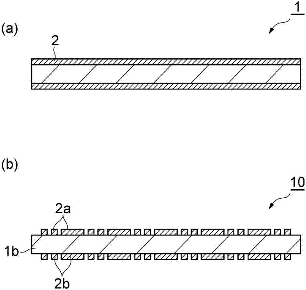
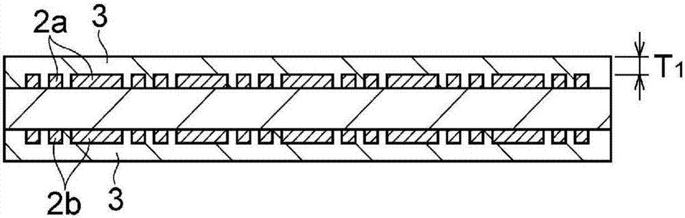
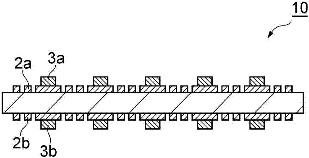
[0055] Refer to the attached Figure 1 Preferred embodiments of the present invention will be described in detail. In the following description, the same or corresponding parts are assigned the same symbols, and repeated descriptions will be omitted. In addition, positional relationships such as up, down, left, and right are based on the positional relationships shown in the drawings unless otherwise specified. Furthermore, the dimensional ratios of the drawings are not limited to the illustrated ratios.

[0056] The method of manufacturing a structure having a conductive circuit according to the present invention is preferably used in the manufacture of a printed wiring board for mounting semiconductor elements. In particular, in addition to being preferably used in the manufacture of printed wiring boards for mounting flip-chip semiconductor elements, it can also be used preferably in coreless substrates, WLP (Wafer Level Package, wafer-level packaging), eWLB (embedded Wa...


PUM

PropertyMeasurementUnit
thicknessaaaaaaaaaa
particle diameteraaaaaaaaaa
particle sizeaaaaaaaaaa

Abstract

A method for manufacturing a structure containing a conductor circuit according to the present invention can provide openings in various shapes by patterning a first photosensitive resin layer in a first patterning process according to shapes of openings formed in a heat-curable resin layer. Further, in the method for manufacturing a structure containing a conductor circuit, a plurality of openings can be formed at the same time and a residue of the resin around the opening can be reduced, unlike a case in which openings are formed with a laser. Therefore, it is possible to sufficiently efficiently manufacture the structure having excellent reliability even when the number of pins of a semiconductor element increases and it is necessary to provide a great number of fine openings.

Description

[0001] This application is a divisional application with the Chinese application number 201280050024.7 filed on October 9, 2012, and the title of the invention is "Structure with Conductor Circuit and Its Manufacturing Method, and Thermosetting Resin Composition". technical field [0002] The present invention relates to a structure having a conductive circuit, a method for producing the same, and a thermosetting resin composition. Background technique [0003] A printed wiring board, which is one of structures having conductive circuits, is a substrate on which a plurality of wiring layers are formed on a core substrate, and includes a copper-plated film laminate serving as a core substrate, and interlayer insulating layers provided between the wiring layers. material and solder resist on the outermost surface. A semiconductor element is usually mounted on a printed circuit board via a die solder material or an underfill material. In addition, if necessary, the entire surf...

Claims


Application Information

Patent Timeline
Patent Type & Authority Applications(China)
IPC IPC(8): H05K3/46C08L79/04C08L63/00C08L63/04C08K9/06C08K3/36C08K3/30H05K3/10
CPCC08J5/18C08K3/30C08K3/36C08K9/06C08L63/00C08L79/04H05K3/4673H05K3/108H05K2203/0582C08K2003/3045C08K2201/003C08J2463/00C08J2479/04C08J2379/04C08J2363/00C08J2363/04C08L63/04Y10T29/49162H05K1/03H05K3/4697G03F7/16G03F7/20G03F7/26G03F7/40H01L21/4857H01L23/49822H01L23/49838H05K3/06H05K3/105
Inventor 蔵渊和彦藤本大辅山田薰平名越俊昌
Owner HITACHI CHEM CO LTD
Why Eureka
Try Eureka