
Organic electroluminescence display device and manufacturing method thereof

A technology of electroluminescent display and manufacturing method, which is applied in the direction of organic semiconductor devices, circuits, electrical components, etc., can solve problems such as failure, device damage, and inability to completely block water vapor, and achieve the effect of reducing impact and prolonging life

Inactive Publication Date: 2017-07-07
SHENZHEN CHINA STAR OPTOELECTRONICS TECH CO LTD
View PDF5 Cites 27 Cited by
  • Summary
  • Abstract
  • Description
  • Claims
  • Application Information

AI Technical Summary

Problems solved by technology

The main method for the industry to improve thin film packaging technology is to use dry sheets or maximize the water and oxygen barrier capacity of the thin film packaging layer, such as depositing multiple layers of organic / inorganic composite films after the display device is manufactured to extend the path of water and oxygen diffusion in the film. However, the technology still has inherent limitations
Because even alternately deposited multi-layer films cannot guarantee that there are no pinholes at all, and the positions where there are pores are often the way for water vapor to infiltrate, which will cause damage or failure of the device.
The industry also uses atomic layer deposition (ALD) to obtain thin films with very few pores. This technology can block water and oxygen, but it cannot completely block water vapor.

Method used


Image

  • Organic electroluminescence display device and manufacturing method thereof
  • Organic electroluminescence display device and manufacturing method thereof

Examples


Embodiment approach

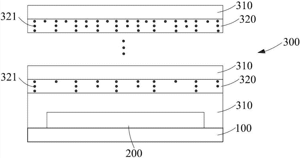
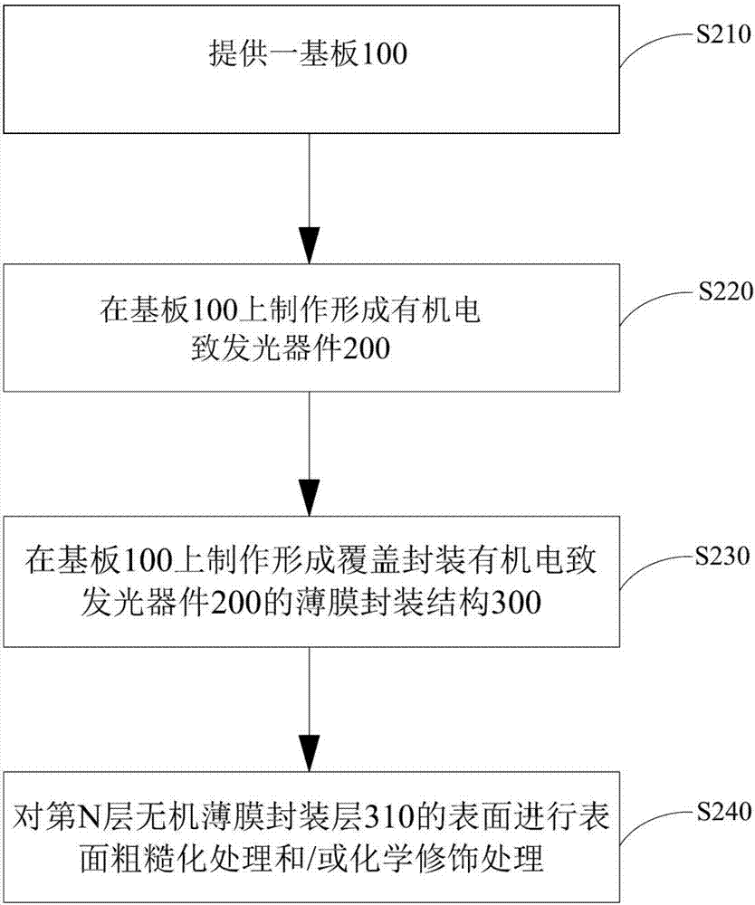
[0036]Here, as an embodiment of the present invention, the method for forming the organic electroluminescent device 200 includes: sequentially forming a bottom electrode, a hole injection layer (HIL), and a hole transport layer (HTL) on the substrate 100 from bottom to top. , light emitting layer (EML), electron transport layer (ETL), electron injection layer (EIL) and top electrode, but the formation method of the organic electroluminescence device of the present invention is not limited to the formation method disclosed here, it can also be is formed using other suitable forming methods.

[0037] S230: Fabricate and form a thin film encapsulation structure 300 covering and encapsulating the organic electroluminescent device 200 on the substrate 100 .

[0038] Here, the method for forming the thin film encapsulation structure 300 includes:

[0039] Firstly, a first inorganic thin film encapsulation layer 310 covering and encapsulating the organic electroluminescence device 2...


PUM


Abstract

The invention provides an organic electroluminescence display device. The organic electroluminescence display device comprises a substrate, an organic electroluminescence device and a thin-film packaging structure, wherein the organic electroluminescence device is arranged on the substrate; the thin-film packaging structure is arranged on the substrate and is used for packaging the organic electroluminescence device, and drying agent particles are arranged in the thin-film packaging structure. The invention also provides a manufacturing method of the organic electroluminescence display device. According to the organic electroluminescence display device and the manufacturing method thereof provided by the invention, the influence of water vapor adsorbed on the surface of a multi-layer packaging thin film or water vapor which has been permeated into the interior of the multi-layer packaging thin film on the packaged organic electroluminescence device can be reduced, so that the service life of the organic electroluminescence device is prolonged.

Description

technical field [0001] The invention belongs to the field of display technology, and in particular relates to an organic electroluminescent display device and a manufacturing method thereof. Background technique [0002] In recent years, organic light-emitting diode (Organic Light-Emitting Diode, OLED) has become a very popular emerging flat-panel display device product at home and abroad, because OLED display device has self-illumination, wide viewing angle, short response time, high luminous efficiency, wide color Domain, low operating voltage, thin thickness, large-size and flexible panels can be produced, and the process is simple, and it also has the potential of low cost. [0003] At present, common packaging technologies for packaging OLED display devices include: glass or metal cover packaging technology with glass substrates, single-layer or multi-layer inorganic thin-film packaging technology, and thin-film packaging technology with alternating organic and inorgani...

Claims


Application Information

Patent Timeline
IPC IPC(8): H01L51/52H01L51/56
CPCH10K59/8731H10K59/874H10K2101/80H10K2102/331H10K50/846H10K50/11H10K50/8445H10K71/00
Inventor 倪奎刘亚伟
Owner SHENZHEN CHINA STAR OPTOELECTRONICS TECH CO LTD
Features
  • Generate Ideas
  • Intellectual Property
  • Life Sciences
  • Materials
  • Tech Scout
  • Unparalleled Data Quality
  • Higher Quality Content
  • 60% Fewer Hallucinations
Learn More