Panel testing device

A panel testing and panel technology, applied in the direction of measuring device, measuring device casing, measuring electricity, etc., can solve the problems of affecting accuracy, detecting bad signal pins, difficulty, etc., to achieve the effect of increasing the width and improving the detection accuracy

Inactive Publication Date: 2017-07-18
BOE TECH GRP CO LTD +1
View PDF7 Cites 5 Cited by
  • Summary
  • Abstract
  • Description
  • Claims
  • Application Information

AI Technical Summary

Problems solved by technology

Taking the current 55" OLED as an example, the resolution is 3840*2160. Since four sub-pixels of RGBW are used to form a pixel (such as figure 2 As shown), so there are 15360 (3840*4) metal wires on the Source side of the data signal input side, which results in a very narrow width and a small distance between the signal Pins on the panel Panel, so that it is necessary to ensure that the test pins on the test block Block are consistent with the It is extremely difficult to correspond the signal pin positions in the panel electrode Pad one by one, which will cause pin misalignment
[0005] image 3 It is a schematic diagram of the alignment situation when the test pin Pin on the test block Block is in the same position as the signal pin Pin in the panel Panel electrode Pad, Figure 4 It is a schematic diagram of pin misalignment when the position of the test pin Pin on the test block Block and the signal pin Pin in the panel electrode Pad are inconsistent. In actual production, Figure 4 It often happens that the misalignment of the test pin Pin on the test block Block and the signal pin Pin in the panel Panel electrode Pad will detect a defect (there is a problem of misjudgment of the signal pin), which will affect the accuracy of judgment

Method used


Image

  • Panel testing device
  • Panel testing device
  • Panel testing device

Examples


Embodiment Construction

[0033] In order to make the purpose, technical solutions and advantages of this document clearer, the embodiments of this document will be described in detail below in conjunction with the accompanying drawings. It should be noted that, in the case of no conflict, the embodiments in the present application and the features in the embodiments can be combined arbitrarily with each other.

[0034] In the following description, a lot of specific details are set forth in order to fully understand this article, but this article can also be implemented in other ways than described here, therefore, the protection scope of this article is not limited by the specific embodiments disclosed below .

[0035] The panel testing device of some embodiments herein will be described below with reference to the accompanying drawings.

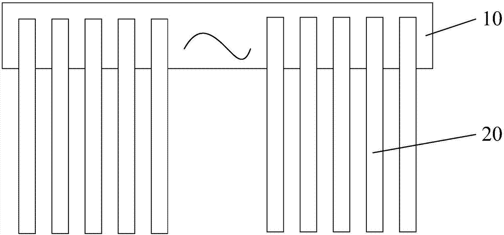
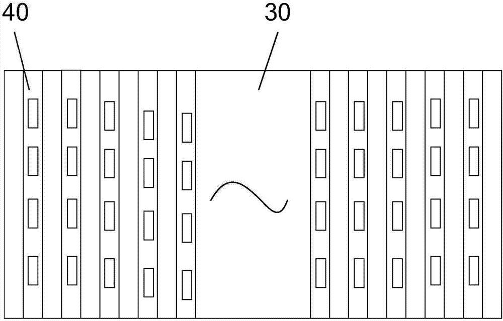
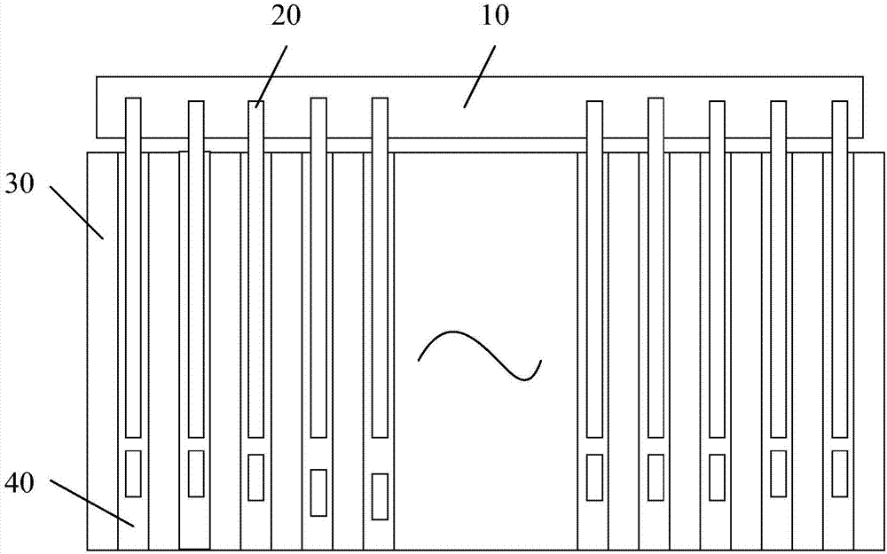
[0036] Panel testing device provided by the present invention, such as Figure 5 , Figure 9 and Figure 10 As shown, it includes: a positioning frame 1; and a...


PUM


Abstract

The invention discloses a panel testing device comprising a positioning rack and a plurality of testing pins transversely arranged on the positioning rack in sequence; the positions of the testing pins are matched with a plurality of signal pins on a to-be-tested panel; a random testing pin complies with the formula: d<=D<=d+L, wherein D refers to the testing pin width, d refers to the width of the signal pin arranged on the to-be-tested panel and matched with the testing pin, L refers to the minimum distance between the signal pin, matched with the testing pin and arranged on the to-be-tested panel, and the adjacent signal pin. The panel testing device can increase the testing pin width, so the signal pin and the testing pin can be better aligned when the panel testing device and the panel are aligned, thus preventing signal pin and testing pin offset conditions, accurately detecting the state of each signal pin, and effectively lifting the signal pin detection accuracy.

Description

technical field [0001] This article involves but is not limited to OLED display technology, especially a panel testing device. Background technique [0002] In the production process of LCD and OLED, the panel after cutting needs to be tested. In order to achieve accurate detection of defects, it is necessary to use full contact detection. Each test pin has a one-to-one correspondence with the signal pins in the Panel electrode Pad; as the resolution of the current panel is getting higher and higher, for example, there are 15360 (3840*4) metal pieces on the Source side of the data signal input side of a 55" OLED line, the accuracy requirements for the one-to-one correspondence between the test block Block and the signal pin Pin in the panel Panel electrode Pad are strict. At present, in actual production, pin misalignment (test pin and signal pin misalignment) is difficult to avoid, which affects the detection Test process. Accuracy of bad detection of signal pins. [0003...

Claims


Application Information

Patent Timeline
Patent Type & Authority Applications(China)
IPC IPC(8): G01R1/04G01R1/067
CPCG01R1/0425G01R1/06716G09G3/006G02F1/136254H10K71/00G09G2320/0693G01R31/3172
Inventor 艾雨谢学武刘博文孙诗刘浩韩坤张阿猛
Owner BOE TECH GRP CO LTD
Why Eureka
Try Eureka