Pixel compensation exposure processing method for microfilming archiving device
A processing method and pixel technology, applied in printing equipment, optics, instruments, etc., can solve the problem of low dpi, achieve the effects of suppressing grids, increasing the number of exposed pixels, and improving the quality of microscopic imaging
- Summary
- Abstract
- Description
- Claims
- Application Information
AI Technical Summary
Problems solved by technology
Method used
Image
Examples
Embodiment
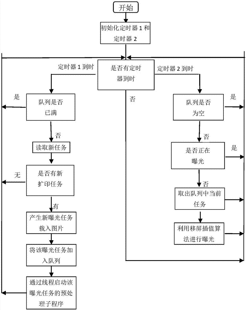
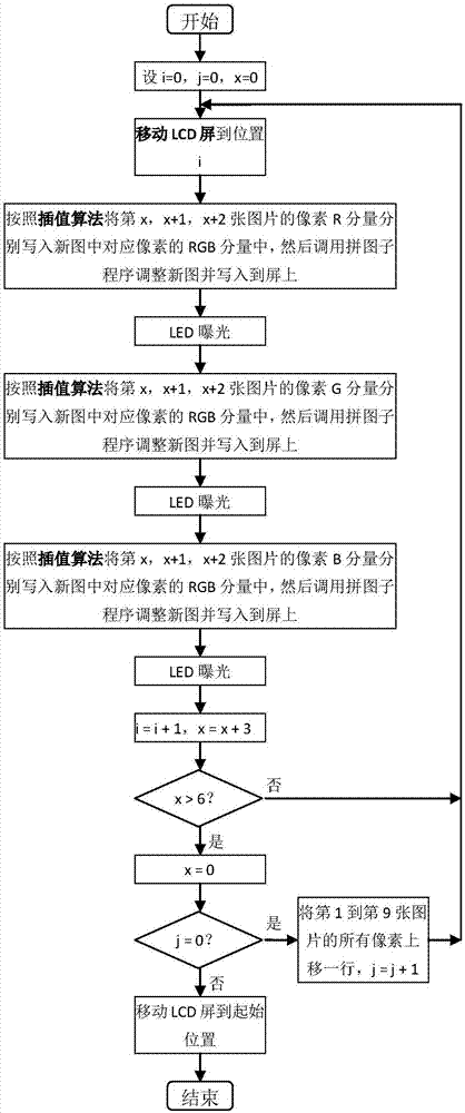
[0092] When using the LCD screen to expose and image, if only relying on the pixels of the screen itself, the number of pixels is not enough; at the same time, there are certain gaps between the pixels on the screen, which leads to grids on the microfilm, in order to make up for this Two defects, the present invention adopts the moving screen interpolation algorithm to solve related problems.
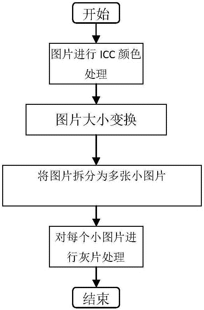
[0093] First, we acquire the image and enlarge it: after 9 exposures, the width and height of the image will be enlarged by 3 times at the same time; and so on.
[0094] Then, we sequentially display the separated small images on the screen for exposure, and at the same time of each exposure, the micro-displacement structure cooperates to move the LCD screen, so that the landing points of multiple exposures of the same pixel point on the LCD screen are evenly filled. In the horizontal and vertical grids generated by the pixel pitch on the screen, we not only increase the number of expos...
PUM
 Abstract
Description
Claims
Application Information


