A Multi-chip Synchronization Architecture Based on Time-to-Digital Converter Circuit

A digital converter and chip technology, applied in electrical digital data processing, instrumentation, signal generation/distribution, etc., can solve the timing deviation of synchronization indication signal, poor waveform quality of synchronization indication signal, and high requirements for driving capability of synchronization indication signal source, etc. problems, to achieve the effect of eliminating transmission delay, reducing load and improving reliability

Active Publication Date: 2019-06-07
NO 24 RES INST OF CETC
View PDF2 Cites 0 Cited by
  • Summary
  • Abstract
  • Description
  • Claims
  • Application Information

AI Technical Summary

Problems solved by technology

However, in the case of a huge number of chips and a high operating frequency, the use of this connection method requires a high driving capability of the synchronous indication signal source, and it is difficult to ensure the transmission path of the synchronous indication signal to each chip for PCB board wiring. same length
Therefore, the timing of the synchronization indication signal received by each chip receiving end will have a large deviation, and because the synchronization indication signal source has too much load, the waveform quality of the synchronization indication signal received by each chip receiving end is poor, resulting in conventional multiple Increased probability of errors in chip synchronization methods

Method used


Image

  • A Multi-chip Synchronization Architecture Based on Time-to-Digital Converter Circuit
  • A Multi-chip Synchronization Architecture Based on Time-to-Digital Converter Circuit
  • A Multi-chip Synchronization Architecture Based on Time-to-Digital Converter Circuit

Examples


Embodiment Construction

[0020] The preferred embodiments of the present invention will be described in detail below in conjunction with the accompanying drawings; it should be understood that the preferred embodiments are only for illustrating the present invention, rather than limiting the protection scope of the present invention.

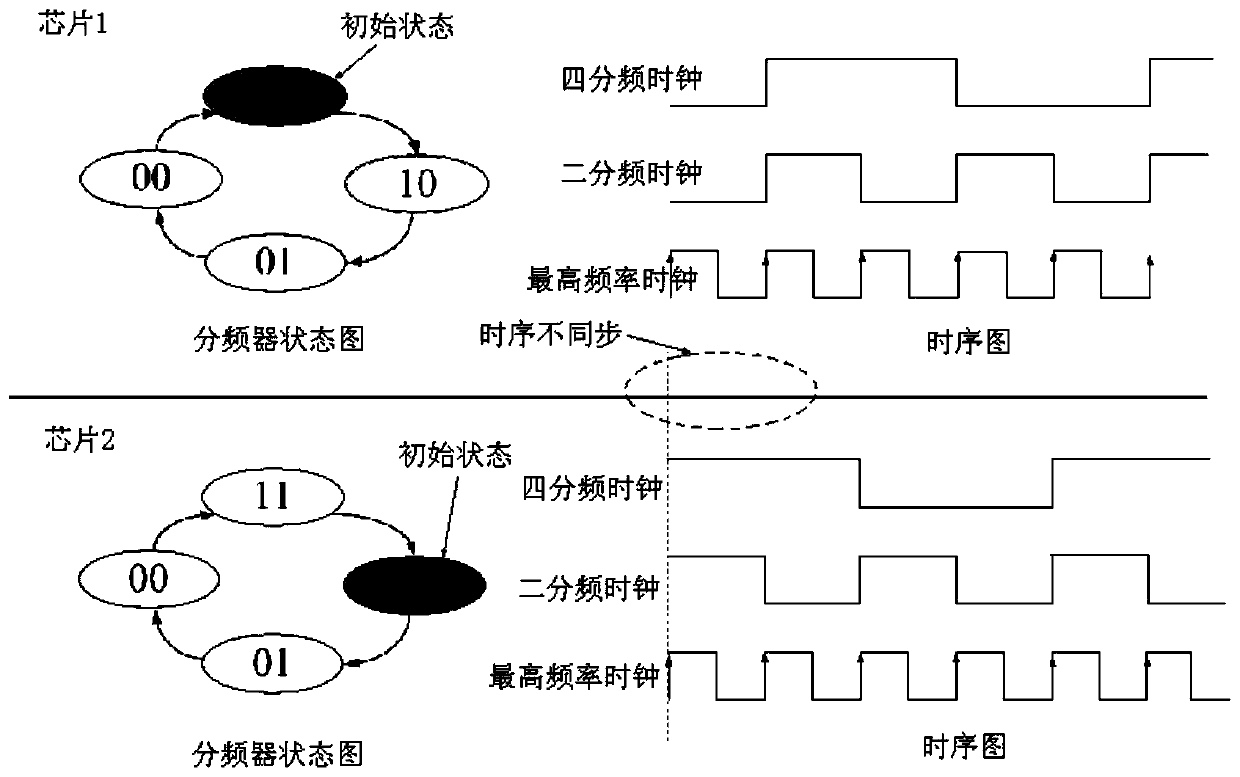
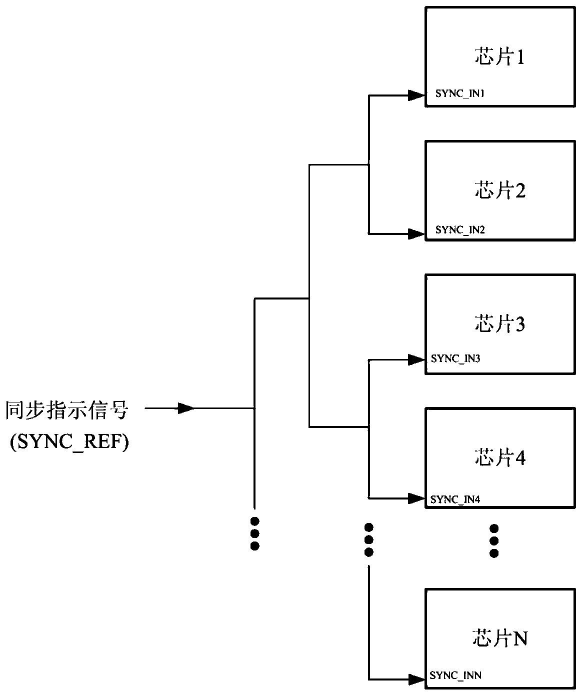
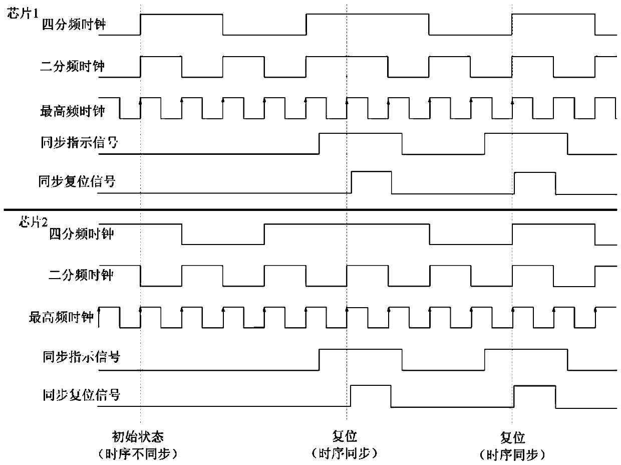
[0021] Such as Figure 4 As shown, a multi-chip synchronization structure based on a time-to-digital converter circuit includes N identical circuit chips with built-in time-to-digital converters and timing adjustment modules.

[0022] The following is an illustration with 3 chips.

[0023] The synchronization indication reference signal (SYNC_REF signal) provided by the whole system is connected to the SYNC_IN1 terminal of the chip 1 and the input terminal of the time-to-digital converter IN1 of the chip 1 . The SYNC_OUT1 terminal of chip 1 is connected to the SYNC_IN2 terminal of chip 2, the input terminal of the time-digital converter IN2 of chip 1 and the input term...


PUM


Abstract

The invention discloses a multichip synchronization structure based on a time-digital converter circuit. The multichip synchronization structure comprises N circuit chips provided with built-in time-digital converters and time sequence regulation modules. Each chip contains a synchronization indicating signal receiving end, a synchronization indicating signal output end, one time-digital converter and one time sequence regulation module, wherein the synchronization indicating signal receiving end is used for receiving a synchronization indicating signal input into the chip externally; the synchronization indicating signal output end is used for outputting a synchronization indicating signal subjected to time sequence resampling through a trigger in the chip, wherein the sampling frequency of the trigger is completely aligned with a time sequence of a maximum frequency clock; the time-digital converter is used for quantizing time sequence delays of two input signals into digital values, wherein the input signal IN1 is the synchronization indicating signal input into the chip externally, and the input signal IN2 is the synchronization indicating signal subjected to time sequence resampling through the trigger in the chip; and the time sequence regulation module is used for regulating output delays of the synchronization indicating signals according to the input digital values. By the adoption of a daisy chain structure, the load on a synchronization indicating signal source is relieved.

Description

technical field [0001] The invention relates to a multi-chip synchronization structure based on a time-to-digital converter circuit. It is directly applied to the multi-chip synchronization function realization in high-speed ADC / DAC and high-speed DDS. Background technique [0002] High-speed DDS and DAC chips need to use multiple sets of clock signals with different frequencies, generally the 2 clock signals with the highest frequency N frequency division generated. Such as figure 1 As shown, taking the frequency division by four as an example, when multiple groups of chips are used at the same time, the initial state of the frequency divider inside the chip is different, which will cause the internal clock timing of multiple groups of chips to be different, so that multiple groups of chips cannot work synchronously. [0003] The connection block diagram of the conventional multi-chip synchronization method is as follows: figure 2 shown. Taking the quarter-frequency a...

Claims


Application Information

Patent Timeline
Patent Type & Authority Patents(China)
IPC IPC(8): G06F1/12G06F13/42
CPCG06F1/12G06F13/4247
Inventor 张俊安张瑞涛付东兵刘军杨毓军罗璞万贤杰李广军
Owner NO 24 RES INST OF CETC
Why Eureka
Try Eureka