Display device

A display device and display panel technology, applied to static indicators, instruments, etc., to improve the overall display quality, provide display uniformity, and reduce flickering effects

Inactive Publication Date: 2017-07-21
KUSN INFOVISION OPTOELECTRONICS
View PDF7 Cites 13 Cited by
  • Summary
  • Abstract
  • Description
  • Claims
  • Application Information

AI Technical Summary

Problems solved by technology

Due to the working principle of the integrated gate drive circuit, the gate voltage received by the gate scan lines of different stages is no longer an ideal constant waveform

Method used


Image

  • Display device
  • Display device
  • Display device

Examples


Embodiment Construction

[0033] Various embodiments of the invention will be described in more detail below with reference to the accompanying drawings. In the various drawings, the same elements are denoted by the same or similar reference numerals. For the sake of clarity, various parts in the drawings have not been drawn to scale.

[0034] The specific implementation manners of the present invention will be further described in detail below in conjunction with the accompanying drawings and embodiments.

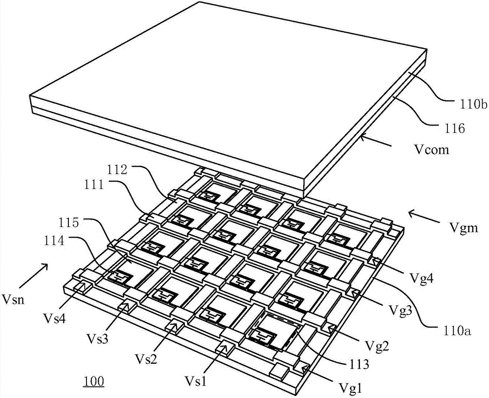
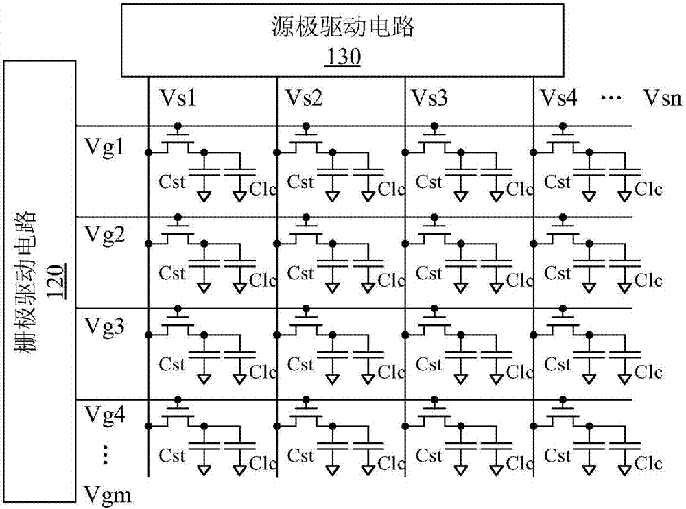
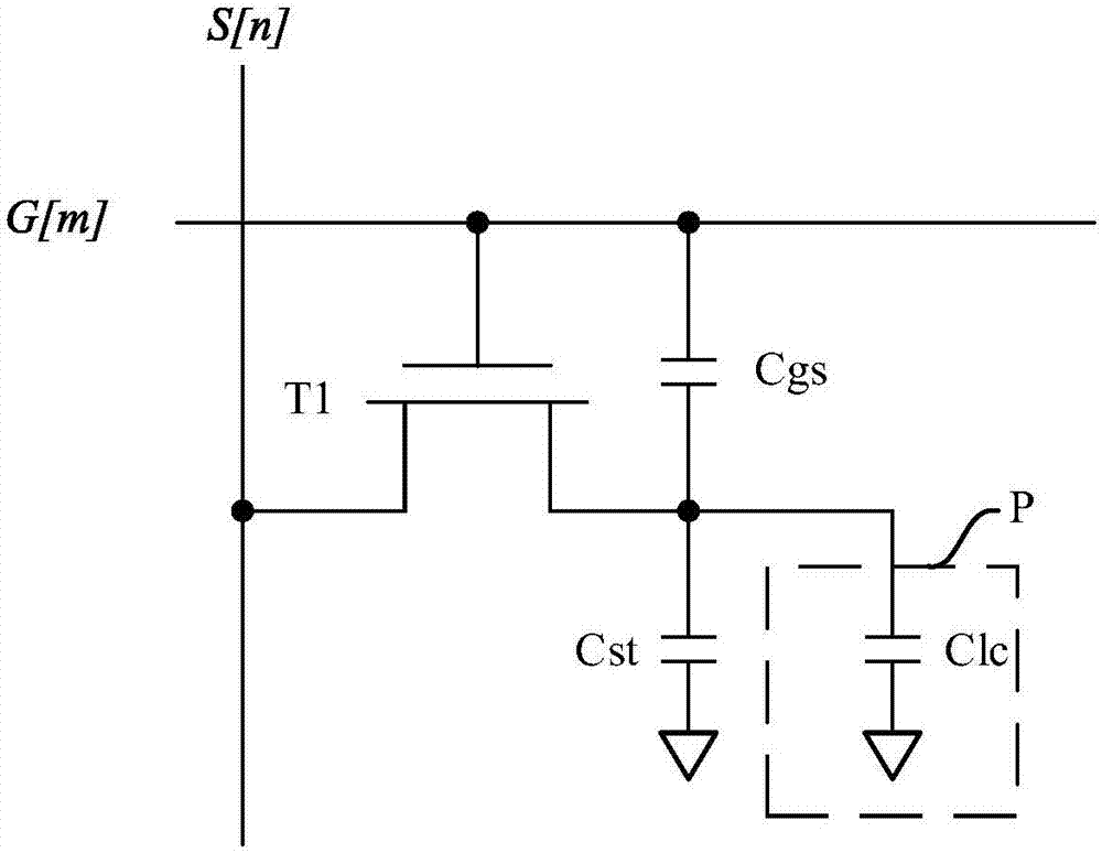
[0035] Figure 5 An equivalent circuit diagram of a display device provided according to an embodiment of the present invention is shown. like Figure 5 As shown, the display device 100 includes a display panel 110 , a gate driving circuit and a source driving circuit 130 integrated on the display panel.

[0036] The display panel 110 includes m gate scanning lines (G[1] to G[m]) 111, n source data lines (S[1]-S[n]) 112, and m ×n pixel units 113, m and n are non-zero natural numbers respective...


PUM


Abstract

The invention discloses a display device comprising a display panel, a grid drive circuit and a source drive circuit. The display panel comprises multiple pixel units which are arranged according to rows and columns, multiple grid scanning lines which are arranged according to the rows, multiple compensation potential lines which are arranged according to the rows and multiple source data lines which are arranged according to the columns. Each pixel unit comprises a thin film transistor, a pixel electrode and a compensation capacitor. The grid drive circuit is used for providing grid voltage to the grid electrodes of the thin film transistors of the pixels of the corresponding row. The source drive circuit is used for providing source voltage to the source electrodes of the thin film transistors of the pixels of the corresponding column so as to set display voltage between the electrode plates of a liquid crystal capacitor. The grid drive circuit comprises multiple grid drive circuits. Each grid drive unit comprises a compensation module and is used for providing compensation voltage to the compensation capacitors of the pixels of the corresponding row in multiple pixels according to a front grid drive signal and a rear grid drive signal. According to the display device, compensation of feed-through voltage can be realized through the grid drive circuit, the compensation capacitors and the compensation potential lines.

Description

technical field [0001] The present invention relates to the field of display technology, and more specifically, to a display device. Background technique [0002] A liquid crystal display device is a display device that uses the phenomenon that the alignment direction of liquid crystal molecules changes under the action of an electric field to change the light transmittance of a light source. Liquid crystal display devices have been widely used in mobile terminals such as cell phones and large-sized display panels such as flat TVs. [0003] figure 1 and 2 A schematic structural diagram and an equivalent circuit diagram of a liquid crystal display device according to the prior art are respectively shown. The liquid crystal display device 100 includes a display panel 110, a first glass substrate 110a and a second glass substrate 110b, the first surface of the first glass substrate 110a is opposite to the first surface of the second glass substrate 110b. A plurality of gate...

Claims


Application Information

Patent Timeline
Patent Type & Authority Applications(China)
IPC IPC(8): G09G3/36
CPCG09G3/3677G09G3/3696G09G2320/0257
Inventor 付佃力房耸赵哲张晋春朱欢欢
Owner KUSN INFOVISION OPTOELECTRONICS
Why Eureka
Try Eureka