Semiconductor circuit arrangement and assembly method with pressurized gel

A circuit layout and semiconductor technology, applied in semiconductor devices, semiconductor/solid-state device manufacturing, semiconductor/solid-state device components, etc., can solve problems such as cracking, non-assemblable parts, and inability to use thermal interface materials

Active Publication Date: 2019-11-15
VINCOTECH
View PDF5 Cites 0 Cited by
  • Summary
  • Abstract
  • Description
  • Claims
  • Application Information

AI Technical Summary

Problems solved by technology

[0011] also, Figure 6 to Figure 9 The known solution shown in has an additional disadvantage: the DCB substrate 206 is under mechanical tension which may cause cracking of the material unless the bend dimensions, bending tool, bending process and material type and layer thickness of the thermal interface material are strictly controlled
[0017] Firstly, this arrangement has the disadvantage that the plastic cover 411 covers parts of the printed circuit board 403, making it impossible to assemble components at these locations
In addition, this package configuration cannot use a hard thermal interface material, such as a phase change material, because the DCB 406 is mechanically weakened due to the opening therein and may crack during the assembly process.

Method used


Image

  • Semiconductor circuit arrangement and assembly method with pressurized gel
  • Semiconductor circuit arrangement and assembly method with pressurized gel
  • Semiconductor circuit arrangement and assembly method with pressurized gel

Examples


Embodiment Construction

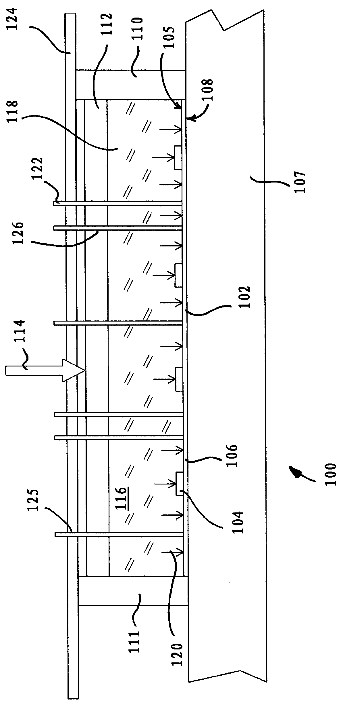
[0060] The invention will now be further described with reference to the accompanying drawings, first with reference to figure 1 . figure 1 A schematic cross-sectional view of a semiconductor circuit arrangement 100 according to the invention is shown.

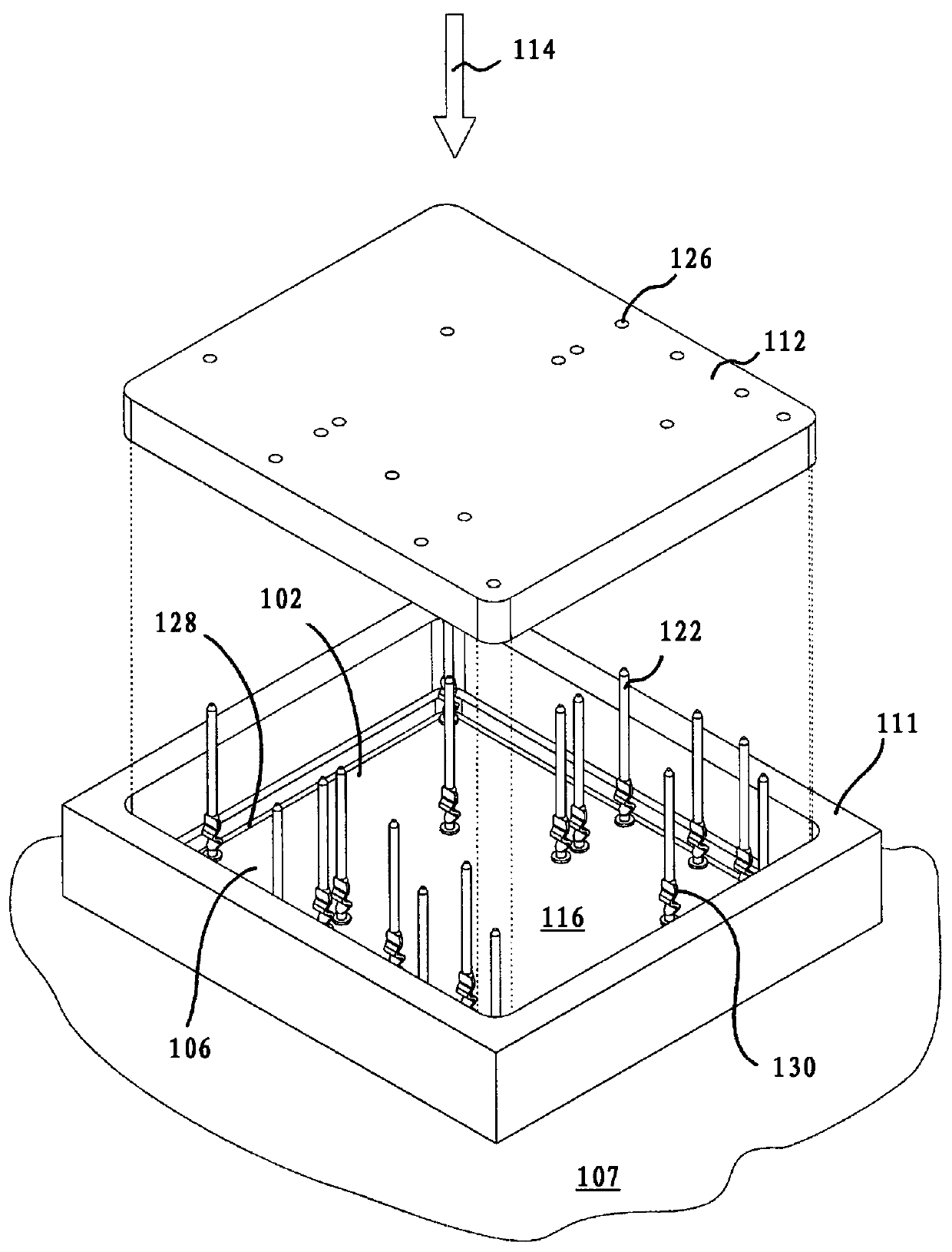
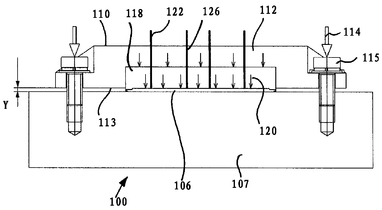
[0061] According to the present invention, the power semiconductor module 102 includes a plurality of semiconductor die 104 mounted on a first surface 105 of a direct copper bonding (DCB) substrate 106 . Via the opposite second surface 108 the DCB substrate 106 is attached to the base plate 107 . Base plate 107 may be made of metal, such as aluminum or copper, and may be connected to a heat sink. alternatively, figure 1 The bottom plate 107 shown may itself represent a heat sink.

[0062] The power semiconductor module 102 is surrounded by a housing 110 , which is made, for example, of a plastic material known in the art. According to the present invention, the housing 110 is formed by a frame 111 and a cover 112 . Cove...


PUM


Abstract

The present invention relates to a semiconductor circuit arrangement and more particularly to a semiconductor circuit arrangement comprising a power semiconductor module. Furthermore, the present invention relates to a method for assembling such a semiconductor circuit arrangement. A semiconductor circuit assembly (100) includes a semiconductor module (102) with at least one electronic component arranged on a first surface of a first circuit carrier, a base plate which is in contact with a second surface of the first circuit carrier, and a housing (110) with a lid (112), the housing (110) being arranged to cover the semiconductor module on the base plate (107). The semiconductor module (102) is at least partially coated with an electrically insulating compressed material (118) covering the at least one electronic component (104), wherein the lid (112) is arranged to impose mechanical pressure on the compressed material (118) in a direction toward said base plate (107).

Description

technical field [0001] The invention relates to semiconductor circuit arrangements and, in particular, to semiconductor circuit arrangements comprising power semiconductor modules. It has to be noted that the principles of the invention can also be applied to packaging any other kind of semiconductor circuits. Furthermore, the invention relates to a method of assembling such a semiconductor circuit arrangement. Background technique [0002] Power semiconductors have become an essential part of every aspect of everyday life. Power semiconductors enable, inter alia, variable speed actuators in consumer goods, industry and transport technology or are part of inverters and rectifiers in the power supply sector. [0003] A problem common to all power semiconductor modules is the relatively high temperature that occurs during operation. Therefore, good thermal contact between the semiconductor power devices and the heat sink for dissipating excess heat is essential for all powe...

Claims


Application Information

Patent Timeline
Patent Type & Authority Patents(China)
IPC IPC(8): H01L23/053H01L23/31H01L23/42H01L25/07
CPCH01L23/053H01L23/3121H01L23/42H01L25/072H01L21/50H01L23/24H01L23/3735H01L23/4006H01L23/49811H01L23/562
Inventor 阿蒂拉·米克洛斯·维格欧托·卡尔马
Owner VINCOTECH
Why Eureka
Try Eureka