A dual-band thin-film photodetector and its preparation method

A photodetector and dual-band technology, which is applied in semiconductor devices, final product manufacturing, sustainable manufacturing/processing, etc., can solve the problems of limited detection band and limited response rate of photodetectors, so as to improve device responsivity, Simple preparation process and good light absorption properties

Active Publication Date: 2018-11-30
HUAZHONG UNIV OF SCI & TECH
View PDF1 Cites 1 Cited by
  • Summary
  • Abstract
  • Description
  • Claims
  • Application Information

AI Technical Summary

Problems solved by technology

[0006] In view of the above defects or improvement needs of the prior art, the present invention provides a dual-band thin-film photodetector and its preparation method. The dual-band thin-film photodetector utilizes a two-dimensional material heterojunction to solve the optical A series of problems such as limited detector responsivity and limited detection band

Method used


Image

  • A dual-band thin-film photodetector and its preparation method

Examples


Embodiment 1

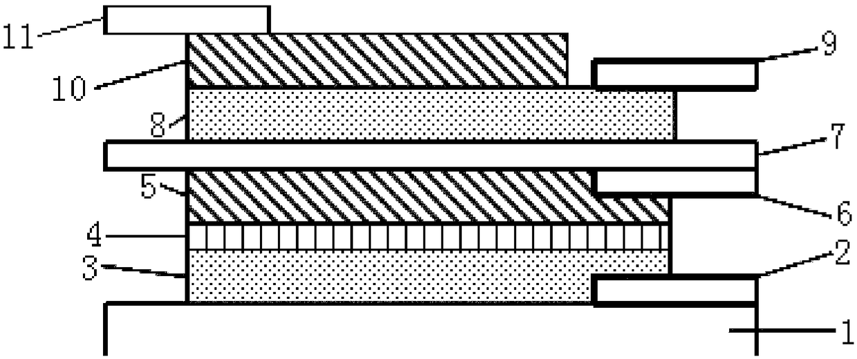
[0044]1) Select silicon wafer, glass or PET plastic as the base sheet 1, clean it, spin-coat photoresist on its surface, and pass photolithography process, figure 1 The photoresist at the position of the middle electrode is washed away after exposure to form grooves.

[0045] 2) Depositing the first electrode layer 2 on the surface of the sample by electron beam evaporation process, the thickness of which is 10 nm.

[0046] 3) Soak the above sample with acetone to remove the remaining photoresist.

[0047] 4) adopt chemical vapor deposition method to prepare graphene thin film on a copper foil, it can be monolayer or several layers, and transfer to the surface of the first electrode layer 2 of step (2) gained; Wherein the transfer method of graphene thin film For: uniformly coating a layer of polymethyl methacrylate film on the surface of the graphene film, then putting it into an etching solution for 4 hours to etch and remove the copper foil, leaving a graphene film support...

Embodiment 2

[0063] 1) Select silicon wafer, glass or PET plastic as the base sheet 1, clean it, spin-coat photoresist on its surface, and pass photolithography process, figure 1 The photoresist at the position of the middle electrode is washed away after exposure to form grooves.

[0064] 2) Depositing the first electrode layer 2 on the surface of the sample by electron beam evaporation process, the thickness of which is 100 nm.

[0065] 3) Soak the above sample with acetone to remove the remaining photoresist.

[0066] 4) adopt chemical vapor deposition method to prepare graphene thin film on a copper foil, it can be monolayer or several layers, and transfer to the surface of the first electrode layer 2 of step (2) gained; Wherein the transfer method of graphene thin film For: the surface of the graphene film is uniformly coated with a layer of polymethyl methacrylate film, then put into an etching solution for 5h to etch and remove the copper foil, leaving a graphene film supported by ...

Embodiment 3

[0082] 1) Select silicon wafer, glass or PET plastic as the base sheet 1, clean it, spin-coat photoresist on its surface, and pass photolithography process, figure 1 The photoresist at the position of the middle electrode is washed away after exposure to form grooves.

[0083] 2) Depositing the first electrode layer 2 on the surface of the sample by electron beam evaporation process, the thickness of which is 200nm.

[0084] 3) Soak the above sample with acetone to remove the remaining photoresist.

[0085] 4) adopt chemical vapor deposition method to prepare graphene thin film on a copper foil, it can be monolayer or several layers, and transfer to the surface of the first electrode layer 2 of step (2) gained; Wherein the transfer method of graphene thin film For: the surface of the graphene film is uniformly coated with a layer of polymethyl methacrylate film, and then put into an etching solution for 4.5h to remove the copper foil by corrosion, leaving a graphene film supp...


PUM


Abstract

The invention belongs to the fields of micro-nano manufacturing and a photoelectronic device, and discloses a dual-wave-band thin film optical detector. The dual-wave-band thin film optical detector comprises a substrate slice, a first electrode layer, a first WSe<2> layer, a graphene layer, a first MoS<2> layer, a second electrode layer, a dielectric layer, a second WSe<2> layer, a third electrode layer, a second MoS<2> layer and a fourth electrode layer, wherein the first electrode layer is arranged on the substrate slice; the first WSe<2> layer is paved on the substrate slice and the first electrode layer; the graphene layer is arranged on the first WSe<2> layer; the first MoS<2> layer is arranged on the graphene layer; the second electrode layer is arranged on the first MoS<2> layer; the dielectric layer is paved on the first MoS<2> layer and the second electrode layer; the second WSe<2> layer is arranged on the dielectric layer; the third electrode layer and the second MoS<2> layer are arranged on the second WSe<2> layer; and the fourth electrode layer is arranged on the second MoS<2> layer. The current carrier adopted by the dual-wave-band thin film optical detector is high in mobility, so that the dual-wave-band thin film optical detector is high in optical absorption characteristic in the visible light wave band.

Description

technical field [0001] The invention belongs to the field of micro-nano manufacturing and optoelectronic devices, and more specifically relates to a dual-band thin-film photodetector and a preparation method thereof. Background technique [0002] Photodetectors are widely used in various fields such as national economy and military affairs. Photodetectors based on detection in different wavelength bands play an important role in the detection of different fields. In the visible and near-infrared bands, photodetectors are mainly used in ray measurement and detection, industrial automatic control, photometric measurement, etc.; in the infrared band, their main uses are missile guidance, infrared imaging, infrared remote sensing, etc.; in the ultraviolet band, The main uses are military applications such as UV guidance, UV warning, UV communication, and UV countermeasures. [0003] The spectral range and detection bandwidth of traditional photodetectors based on group IV and ...

Claims


Application Information

Patent Timeline
Patent Type & Authority Patents(China)
IPC IPC(8): H01L31/109H01L31/032H01L31/028H01L31/20
CPCH01L31/028H01L31/032H01L31/109H01L31/20H01L31/202Y02P70/50
Inventor 廖广兰孙博吴悠妮史铁林谭先华刘智勇汤自荣
Owner HUAZHONG UNIV OF SCI & TECH
Why Eureka
Try Eureka