Liquid crystal display device

A technology of liquid crystal display device and display area, which is applied in the directions of instruments, nonlinear optics, optics, etc., can solve the problems of intrusion, disconnection of signal lines, damage of TFT elements of display pixels, etc.

Inactive Publication Date: 2017-08-18
MITSUBISHI ELECTRIC CORP
View PDF14 Cites 10 Cited by
  • Summary
  • Abstract
  • Description
  • Claims
  • Application Information

AI Technical Summary

Problems solved by technology

[0010] However, in Patent Document 3, since the inspection pad is used as a ground electrode, although it is added through the switching element, it is connected to the panel display part, so when the charge enters CF, conductive paste, etc. due to static electricity, etc. In the case of conductive tape, etc., it may invade the display area through the signal line, causing damage to the TFT element of the display pixel and disconnection of the signal line

Method used


Image

  • Liquid crystal display device
  • Liquid crystal display device
  • Liquid crystal display device

Examples


Embodiment approach 1

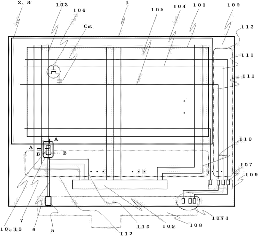
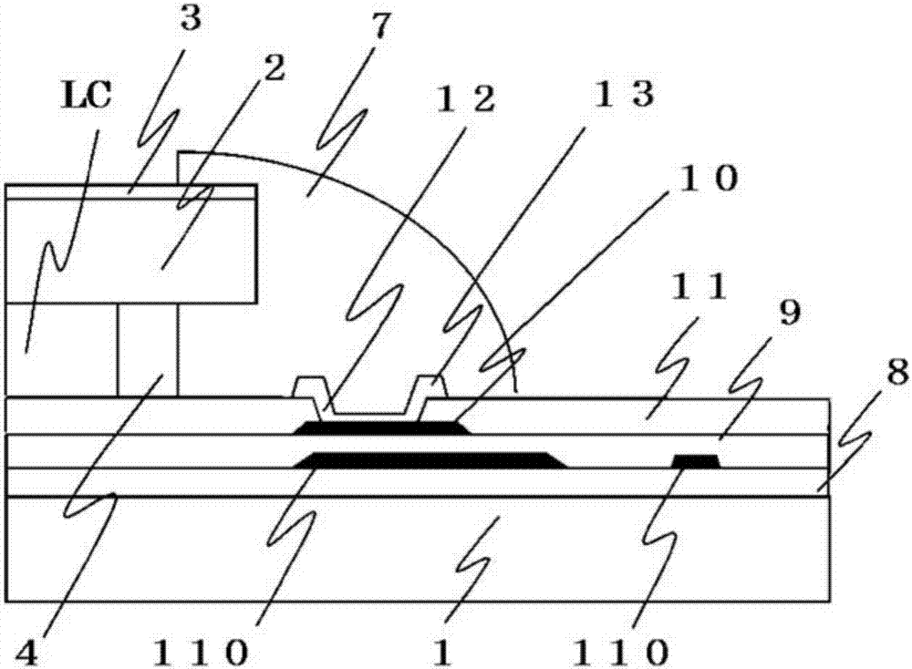
[0037] Hereinafter, embodiments of the present invention will be described using the drawings. figure 1 It is a plan view of the liquid crystal display panel of the liquid crystal display device according to the embodiment. in addition, figure 2 is a cross-sectional view of a liquid crystal display panel, specifically, a figure 1 Sectional view of the part shown in A-A. All the drawings are schematic diagrams, and do not reflect the exact size and the like of the illustrated components. In addition, omission of description, simplification of a part of the structure, etc. are suitably performed about the parts other than the main part of the invention for easy understanding of the drawings.

[0038] like figure 1 , 2 As shown, in the liquid crystal display panel 100, a TFT substrate 1, which is a first substrate on which wiring and the like are formed, and a CF (color filter) substrate 2, which is a second substrate opposite thereto, are used to encapsulate liquid crystal...

Embodiment approach 2

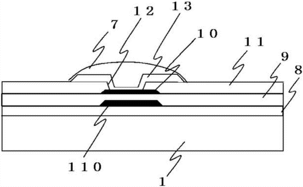
[0075] In the display area 101 of Embodiment 1, a new second common wiring (not shown) may be provided on the same layer as the scanning line 104, and the common wiring 105 on the capacitive insulating film 27 and the second 2. The common wiring is electrically connected through a contact hole (not shown) opened in the insulating film. With this structure, since the resistance of the common wiring can be reduced, there is an effect of improving the display quality. In addition, in this case, the lead-out wiring 111 may be formed by extending the second common wiring of the same layer as the scanning line 104 .

[0076] In the case where the common wiring 105 is directly led out to constitute the lead wiring 111 , if it is attempted to provide the ground electrode 10 thereon, it is necessary to further form an insulating film covering the common wiring 105 . However, if the second common wiring, the lead-out wiring 111 connected to the second common wiring, and the scanning li...

Embodiment approach 3

[0079] In Embodiment 2, the second common wiring is formed on the same layer as the scanning line, but the layer to which the second common wiring is added is not limited to the same layer as the scanning line 104 , and may be laminated with the common wiring 105 . And, as otherwise, except Figure 4 , Figure 5 In addition to the illustrated form, a second common wiring made of a metal film may be separately formed on the same layer as the pixel electrode. In this case, the second common wiring may be electrically connected to the common wiring on the capacitive insulating film via a contact hole. With this structure, since the resistance of the common wiring can be reduced, there is also an effect of improving the display quality.

[0080] In addition, in the case where the second common wiring is formed by a metal film, if it is formed so as to overlap with at least one of the scanning line 104 or the signal line 103, there is an effect that the use of the pixel portion w...


PUM


Abstract

A liquid crystal display device includes: a first substrate which includes a display region, in which scan wirings and signal wirings intersecting with scan wirings are formed, and a frame region, which surrounds the display region, wherein a lead-out wiring 110 extending from at least one of the signal wiring and the scan wiring and a ground electrode 10 on an insulating layer covering the lead-out wiring are formed in the frame region 102; a second substrate, which faces the first substrate with interposing a seal, wherein a transparent conductive film is formed on a surface opposite to a side where the liquid crystal is provided; and a conductive member 7, which is formed to extend across the first substrate and the second substrate to electrically connect the transparent conductive film 7 with the ground electrode 10, wherein the ground electrode 10 overlaps with at least one of the lead-out wirings.

Description

technical field [0001] The invention relates to a liquid crystal display device. Background technique [0002] For electro-optical display devices, especially IPS (In Plane Switching, In Plane Switching) mode, FFS (Fringe Field Switching, Fringe Field Switching) mode liquid crystal display devices, the display quality is reduced due to the charge generated on the display surface of the display panel. , so the charge needs to be released. For this reason, the display surface of the display panel and the electrodes provided on the TFT substrate are often electrically connected using a conductive tape or a conductive paste, as in, for example, the device described in Patent Document 1. [0003] In the terminal region of the device described in Patent Document 1, ID pads, driver ICs, FPC (Flexible Printed Circuit) and the like need to be arranged in addition to electrodes for grounding. Therefore, as the frame narrowing progresses, it becomes difficult to design a pattern that...

Claims


Application Information

Patent Timeline
Patent Type & Authority Applications(China)
IPC IPC(8): G02F1/1362G02F1/1343
CPCG02F1/134309G02F1/136227G02F1/136286G02F1/136204G02F2202/22G02F1/134363G02F1/134372G02F1/133345G02F1/1368G02F1/13439G02F1/1339G02F2201/123
Inventor 平田直也上野孝弘
Owner MITSUBISHI ELECTRIC CORP
Why Eureka
Try Eureka