Wafer-level chip packaging structure and packaging method

A wafer-level chip and packaging structure technology, applied in radiation control devices, electrical components, electrical solid devices, etc., can solve problems such as increase, insufficient chip edge strength, and risks

Inactive Publication Date: 2017-08-18
MICROARRAY MICROELECTRONICS CORP LTD
View PDF3 Cites 2 Cited by
  • Summary
  • Abstract
  • Description
  • Claims
  • Application Information

AI Technical Summary

Problems solved by technology

[0003] However, some chips (such as capacitive fingerprint sensor chips) require TSV packaging but do not have a glass plate as a support in order to reduce the thickness of the package. structure), will produce technical defects of in...

Method used


Image

  • Wafer-level chip packaging structure and packaging method
  • Wafer-level chip packaging structure and packaging method
  • Wafer-level chip packaging structure and packaging method

Examples


Embodiment Construction

[0030] In order to enable those skilled in the art to better understand the technical solutions in the present invention, the technical solutions in the embodiments of the present invention will be clearly and completely described below in conjunction with the drawings in the embodiments of the present invention. Obviously, the described The embodiments are only some of the embodiments of the present invention, not all of them. Based on the embodiments of the present invention, all other embodiments obtained by persons of ordinary skill in the art without making creative efforts shall fall within the protection scope of the present invention.

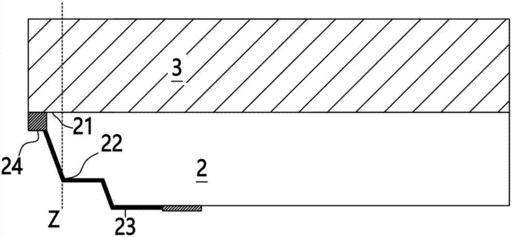
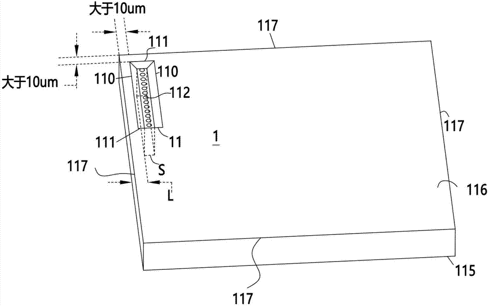
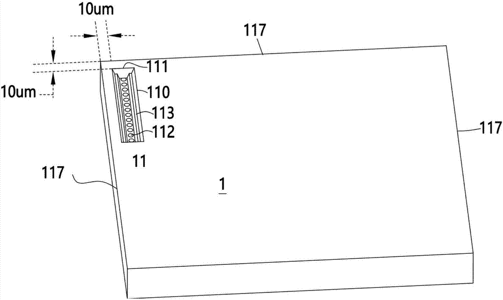
[0031] Such as Figure 2a As shown, the wafer-level chip packaging structure of the present invention includes a chip unit 1 , and the chip unit has a first surface 115 and a second surface 116 disposed opposite to each other. In the present invention, the fingerprint sensor chip is taken as an example, the first surface 115 is provide...


PUM


Abstract

The invention relates to a wafer-level chip packaging structure and packaging method. The wafer-level chip packaging structure includes a chip unit provided with a first surface and a second surface arranged oppositely. The first surface is provided with at least one welding window used for electric connection. The second surface is provided with a TSV structure connected with the welding window. The TSV structure includes a through hole penetrating the first surface and the second surface and a slot arranged in the second surface. The boundary of the slot is greater 10 micrometers away from the edge of the second surface. Compared with the prior art, the progress is that the structural strength of a chip is improved.

Description

technical field [0001] The invention relates to the technical field of semiconductors, in particular to a wafer-level chip packaging structure and a packaging method thereof. Background technique [0002] TSV (Through Silicon Vias) packaging structure is a kind of IC packaging method, which can be divided into memory packaging and wafer-level packaging for chip devices. Wafer-level packaging is used on optical image sensors (please refer to figure 1 ), in this case, the optical image sensor 2 has a glass substrate 3 supporting the TSV structure 4 to maintain structural strength, and Z-axis connection structures such as TSV openings 41, slots 22, wiring 23 and soldering windows 24 are arranged on the edge of the image sensor chip 21 to facilitate fabrication. [0003] However, some chips (such as capacitive fingerprint sensor chips) require TSV packaging but do not have a glass plate as a support in order to reduce the thickness of the package. structure), will produce tec...

Claims


Application Information

Patent Timeline
IPC IPC(8): H01L23/535H01L23/528H01L21/56H01L27/146
CPCH01L21/561H01L23/528H01L23/535H01L27/14683
Inventor 蒋舟李扬渊
Owner MICROARRAY MICROELECTRONICS CORP LTD
Why Eureka
Try Eureka