Low-cost intelligent chip carrier band and manufacturing method therefor

A smart chip, low-cost technology, applied in semiconductor/solid-state device manufacturing, electrical components, electric solid-state devices, etc., can solve the problems of cavity deformation, low mold coverage rate, high price, etc., to reduce manufacturing cost and material cost , cost reduction effect

Pending Publication Date: 2017-08-22
新恒汇电子股份有限公司
View PDF0 Cites 2 Cited by
  • Summary
  • Abstract
  • Description
  • Claims
  • Application Information

AI Technical Summary

Problems solved by technology

However, the mold design is complicated, and the versatility of the mold is low for different products. Different products basically need to customize different molds to match them. The price is high, and the process control is difficult, the mold coverage rate is low, and the material at the cavity position is soft. , when the force is uneven, it is easy to cause the deformation of the cavity, resulting in a decrease in yield

Method used


Image

  • Low-cost intelligent chip carrier band and manufacturing method therefor
  • Low-cost intelligent chip carrier band and manufacturing method therefor
  • Low-cost intelligent chip carrier band and manufacturing method therefor

Examples


Embodiment Construction

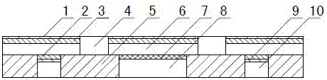
[0034] Figure 1~11 It is the best embodiment of the present invention, below in conjunction with attached Figure 1~11 The present invention will be further described.

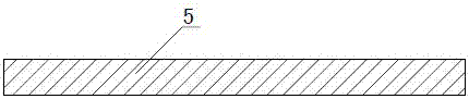
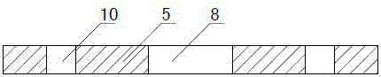
[0035] Such as figure 1 As shown, a low-cost smart chip carrier tape includes a carrier tape base material 5, and a plurality of contact blocks are formed on the upper surface of the base tape base material 5 through insulating grooves 4. The combined copper foil layer 6 and the contact nickel layer 3 and the contact gold layer 1 above the copper foil layer 6. A cavity 8 is opened in the middle of the lower surface of the carrier tape substrate 5, and a welding hole 10 corresponding to the contact block is provided on the outer ring of the cavity 8, and the copper foil layer corresponding to the corresponding position is covered in the welding hole 10. The welded nickel layer 2 bonded to 6 and the welded nickel layer 2 are covered with an insulating layer 7 bonded to the copper foil layer 6 at the corresp...


PUM


Abstract

The invention discloses a low-cost intelligent chip carrier band and a manufacturing method therefor, and belongs to the technical field of intelligent chip packaging. The low-cost intelligent chip carrier band comprises a carrier band base material (5); a surface conductive layer is formed on the upper surface of the carrier band base material (5); the surface conductive layer is divided into multiple contact blocks at intervals by insulating trenches (4); the surface metal layer comprises a bottom metal layer and a contact metal layer arranged on the upper surface of the bottom metal layer; the low-cost intelligent chip carrier band is characterized in that welding holes (10) corresponding to the contact blocks are formed in the lower surface of the carrier band base material (5); an intra-hole metal layer fitted with the surface conductive layer is formed in the welding holes (10); a cavity hole (8) is formed in the middle part of the carrier band base material (5); and an insulating layer is arranged on the upper surface of the cavity hole (8). According to the low-cost intelligent chip carrier band and the manufacturing method therefor, the intra-hole metal layer is not formed in the cavity hole for fixing chips, so that the cost is greatly lowered.

Description

technical field [0001] A low-cost intelligent chip carrier tape and a manufacturing method belong to the technical field of intelligent chip packaging. Background technique [0002] With the development of integrated circuits and the improvement of people's living standards, the application of smart cards has become more and more extensive. It has been widely used in telecommunications, banking, social security, logistics and other fields. The general process of the smart card is: fix the chip on the carrier tape, then weld the terminals on the chip and the corresponding terminals on the carrier tape, and then solidify and package the chip and its surrounding welding wires. [0003] In recent years, under the market prospect of miniaturization of electronic products, the thinning of smart cards has become a current trend. In order to reduce the package height of the module, an accommodating cavity for placing the chip is opened on the carrier tape, and the chip is fixed in ...

Claims


Application Information

Patent Timeline
IPC IPC(8): H01L21/50H01L21/52H01L21/673
CPCH01L21/50H01L21/52H01L21/67356H01L2221/683Y02P70/50
Inventor 陈庆颖王广南张成彬
Owner 新恒汇电子股份有限公司
Why Eureka
Try Eureka