Shifting registration unit and driving method thereof, and display panel

A technology of shift register units and transistors, which is applied in information storage, static memory, static indicators, etc., and can solve problems such as output instability

Inactive Publication Date: 2017-08-29
SHANGHAI TIANMA AM OLED
View PDF10 Cites 18 Cited by
  • Summary
  • Abstract
  • Description
  • Claims
  • Application Information

AI Technical Summary

Problems solved by technology

[0004] Embodiments of the present invention provide a shift register unit, its driving method,

Method used


Image

  • Shifting registration unit and driving method thereof, and display panel
  • Shifting registration unit and driving method thereof, and display panel
  • Shifting registration unit and driving method thereof, and display panel

Examples


example 1

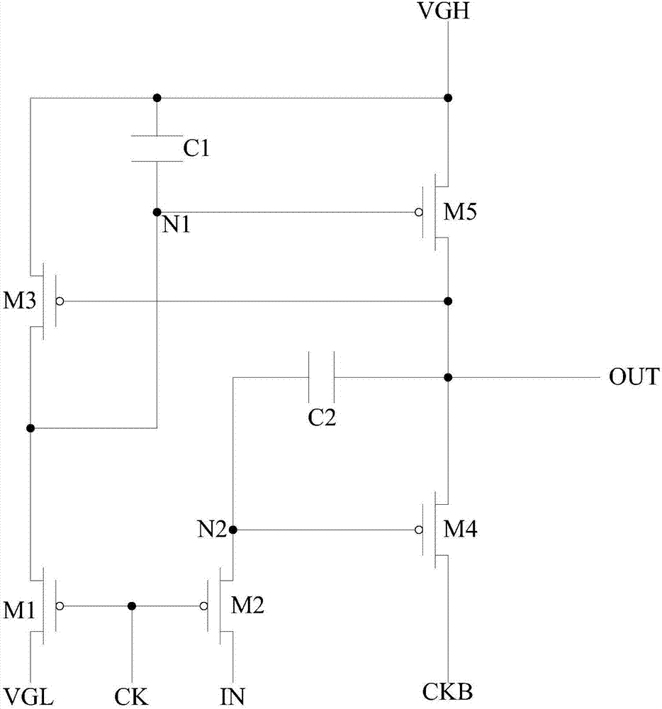
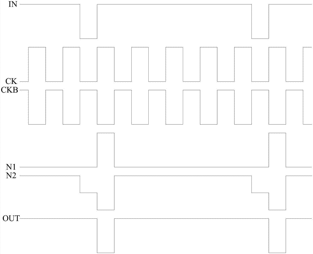
[0087] by Figure 3a and Figure 5a Take the shift register unit shown as an example, all transistors in the shift register unit are P-type transistors, and the corresponding input and output timings are as follows: Figure 7a as shown, Figure 7a An input and output timing diagram corresponding to the shift register unit provided by the embodiment of the present invention; specifically, select as Figure 7a T1, T2, T3, T4 and T5 five stages in the input timing diagram shown.

[0088] In the T1 stage, IN=1, CK=0, and CKB=1.

[0089] Because CK=0, the first transistor T1 and the second transistor T2 are turned on; because CKB=1, the fifth transistor T5 is turned off; because the first signal terminal V1 is at low level, the fourth transistor T4 is turned on. The turned-on first transistor T1 transmits the high-level signal of the input signal terminal IN to the first node N1, so the first node N1 is high-level, and the third transistor T3 is turned off; the high-level signa...

example 2

[0105] by Figure 4a and Figure 6a Take the shift register unit shown as an example, all transistors in the shift register unit are P-type transistors, and the corresponding input and output timings are as follows: Figure 7a as shown, Figure 7a An input and output timing diagram corresponding to the shift register unit provided by the embodiment of the present invention; specifically, select as Figure 7a T1, T2, T3, T4 and T5 five stages in the input timing diagram shown.

[0106] specifically, Figure 4a The shift register unit shown with the Figure 3a Compared with the shift register unit shown, there is an arrangement of the sixth transistor, Figure 6a The shift register unit shown with the Figure 5aCompared with the shown shift register unit, the setting of the sixth transistor is added, so the specific working principle is basically the same.

[0107] In the T1 stage, IN=1, CK=0, and CKB=1.

[0108] Because CK=0, the first transistor T1 and the second trans...

example 3

[0124] by Figure 3b and Figure 5b Take the shift register unit shown as an example, all transistors in the shift register unit are N-type transistors, and the corresponding input and output timing is as follows Figure 7b as shown, Figure 7b An input and output timing diagram corresponding to the shift register unit provided by the embodiment of the present invention; specifically, select as Figure 7b T1, T2, T3, T4 and T5 five stages in the input timing diagram shown.

[0125] In the T1 stage, IN=0, CK=1, and CKB=0.

[0126] Because CK=1, the first transistor T1 and the second transistor T2 are turned on; because CKB=0, the fifth transistor T5 is turned off; because the first signal terminal V1 is at a high level, the fourth transistor T4 is turned on. The turned-on first transistor T1 transmits the low-level signal of the input signal terminal IN to the first node N1, so the first node N1 is low-level, and the third transistor T3 is turned off; the low-level signal o...


PUM


Abstract

The present invention discloses a shifting registration unit and a driving method thereof, and a display panel. The unit comprises an input module, a first control module, a second control module, a feedback regulation module, an output module, a first coupling module and a second coupling module. The feedback regulation module is configured to feed back signals of an output signal end to a first node under the control of a second clock signal end, the second control module allows the first node to conduct with a third node under the control of first signals to reduce the suspension time of the third node; the first control module provides signals of the first clock signal end or a first signal end to a second node under the control of the first clock signal end to reduce the suspension time of the second node; and because the suspension time of the second node and the third node are short, a circuit does not has the node potential competition problem, and therefore the anti-interference performance of the shifting registration unit is high, and the output is stable.

Description

technical field [0001] The invention relates to the field of display technology, in particular to a shift register unit, its driving method and a display panel. Background technique [0002] With the continuous development of display screens, consumers have higher and higher requirements for the stability of display screens. The stability of the display screen is largely reflected in the gate drive circuit and the shift register unit forming the gate drive circuit. [0003] Currently, the shift register unit mostly adopts a 5T2C structure (that is, includes 5 switching transistors and 2 capacitors). Such as Figure 1a as shown, Figure 1a A schematic structural diagram of a shift register unit provided in the prior art; the first switching transistor M1 to the fifth switching transistor M5 are all P-type thin film transistors. Such as Figure 1b shown in the circuit timing diagram, Figure 1b for Figure 1a The circuit timing diagram corresponding to the shift register u...

Claims


Application Information

Patent Timeline
IPC IPC(8): G09G3/20G11C19/28
CPCG09G3/20G11C19/28G09G2310/0267G09G2310/0286G11C19/287G09G3/3677G09G5/006G09G2310/08
Inventor 朱仁远
Owner SHANGHAI TIANMA AM OLED
Why Eureka
Try Eureka