Organic light-emitting diode (OLED) display panel encapsulation structure, manufacturing method of OLED display panel encapsulation structure, and display device

A technology of light-emitting diodes and display panels, which is applied in the manufacture of semiconductor/solid-state devices, semiconductor devices, electrical components, etc., and can solve the problems of reducing the service life of organic light-emitting diode devices, easily breaking glass retaining walls, and easily reducing adhesion, etc. Achieve the effects of improving packaging reliability, improving bonding reliability, and prolonging service life

Active Publication Date: 2017-08-29
BOE TECH GRP CO LTD +1
View PDF7 Cites 17 Cited by
  • Summary
  • Abstract
  • Description
  • Claims
  • Application Information

AI Technical Summary

Problems solved by technology

[0004] However, the glass barrier is easily broken when subjected to external pressure, and, as the forming material of the glass barrier ages, the adhesion between the glass barrier and the organic light-emitting diode display substrate and the glass cover is also easily reduced, making the glass barrier Cracks appear where the wall overlaps the organic light emitting diode display substrate and glass cover, causing external water and oxygen to penetrate into the organic light emitting diode device, thereby reducing the service life of the organic light emitting diode device

Method used


Image

  • Organic light-emitting diode (OLED) display panel encapsulation structure, manufacturing method of OLED display panel encapsulation structure, and display device
  • Organic light-emitting diode (OLED) display panel encapsulation structure, manufacturing method of OLED display panel encapsulation structure, and display device
  • Organic light-emitting diode (OLED) display panel encapsulation structure, manufacturing method of OLED display panel encapsulation structure, and display device

Examples


Embodiment Construction

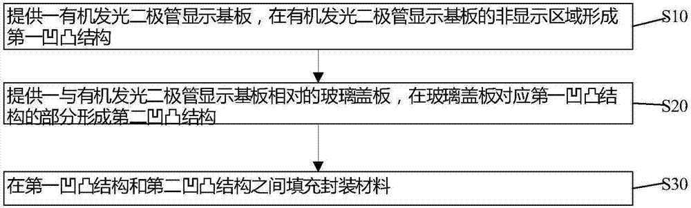
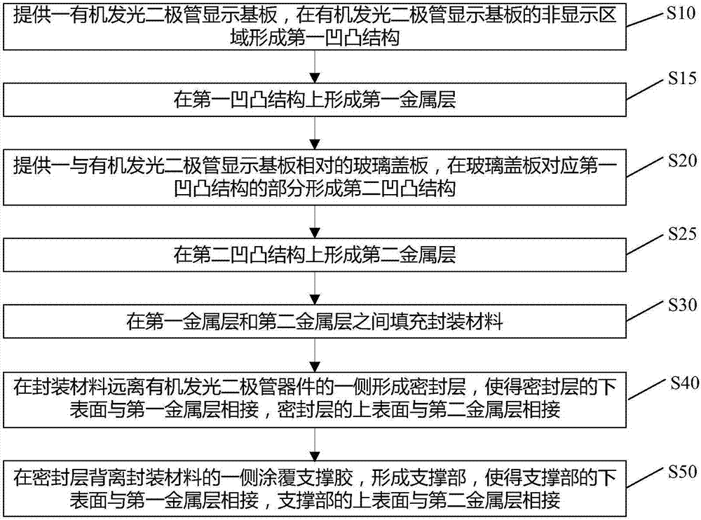
[0029] In order to further illustrate the packaging structure of the organic light emitting diode display panel provided by the embodiments of the present invention, its manufacturing method, and the display device, a detailed description will be given below in conjunction with the accompanying drawings.

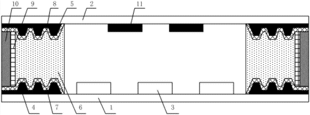
[0030] refer to figure 1 , the organic light emitting diode display panel packaging structure provided by the embodiment of the present invention includes an organic light emitting diode display substrate 1 and a glass cover plate 2 arranged oppositely, the non-display area of ​​the organic light emitting diode display substrate 1 and the corresponding non-display area of ​​the glass cover plate 2 An encapsulation part is provided between the parts, and the organic light emitting diode device 3 of the organic light emitting diode display substrate 1 is located in a sealed cavity surrounded by the organic light emitting diode display substrate 1, the glass cover plate 2 and th...


PUM


Abstract

The invention relates to the field of display technologies, and discloses an organic light-emitting diode (OLED) display panel encapsulation structure, a manufacturing method of the OLED display panel encapsulation structure, and a display device, which are used to improve the sealing reliability of OLED device encapsulation and prolong the service life of OLED devices. The OLED display panel encapsulation structure comprises an OLED display substrate and a glass cover plate which are oppositely arranged, wherein encapsulation parts are arranged between non-display areas of the OLED display substrate and parts of the glass cover plate corresponding to the non-display areas; and each encapsulation part comprises a first concave-convex structure arranged on the OLED display substrate, a second concave-convex structure arranged on the glass cover plate, and encapsulation materials arranged between the first concave-convex structure and the second concave-convex structure. The OLED display panel encapsulation structure, the manufacturing method of the OLED display panel encapsulation structure, and the display device provided by the invention are used for an OLED display device.

Description

technical field [0001] The invention relates to the field of display technology, in particular to an organic light emitting diode display panel packaging structure, a manufacturing method thereof, and a display device. Background technique [0002] Organic Light Emitting Diode (OLED) devices are widely used in the display industry due to their advantages of high brightness, full viewing angle, fast response and flexible display. However, since the organic light emitting diode device is very sensitive to water and oxygen in the air, the water and oxygen that penetrate into the organic light emitting diode device will seriously affect the service life of the organic light emitting diode device. Therefore, the organic light emitting diode device needs to use The encapsulation structure is used for encapsulation, so as to block water, oxygen, etc. by using the encapsulation structure. [0003] At present, laser glass encapsulation (Frit encapsulation) is a commonly used encapsu...

Claims


Application Information

Patent Timeline
Patent Type & Authority Applications(China)
IPC IPC(8): H01L51/52
CPCH10K50/8423H10K50/8426H10K50/844H10K59/12H10K50/865H10K59/00H10K71/00
Inventor 吴守政张青黄甫升邵吉刘大鹏欧阳志刚王小俊许军殷宝清
Owner BOE TECH GRP CO LTD
Why Eureka
Try Eureka