Machining process of PCB

A PCB board and processing technology technology, applied in the field of PCB board processing technology, can solve the problems of single-sided opening of solder mask holes, contaminated pads, and rising processing costs.

Inactive Publication Date: 2017-09-01
珠海杰赛科技有限公司 +1
View PDF3 Cites 5 Cited by
  • Summary
  • Abstract
  • Description
  • Claims
  • Application Information

AI Technical Summary

Problems solved by technology

[0003] The technical problem to be solved by the present invention is to provide a PCB board processing technology to solve the problem that the PCB product design solder resist plug holes need to be repaired by opening windows on one side or by opening windows in local locations to pollute the solder pads, and solve the problem that direct use of solder resist plug holes does not need to be repaired. The problem of rising processing costs caused by changing to resin plug holes to solve the above-mentioned multiple defects caused by the prior art

Method used


Image

  • Machining process of PCB
  • Machining process of PCB
  • Machining process of PCB

Examples


Embodiment 1

[0027] A PCB board processing technology, comprising the following process steps,

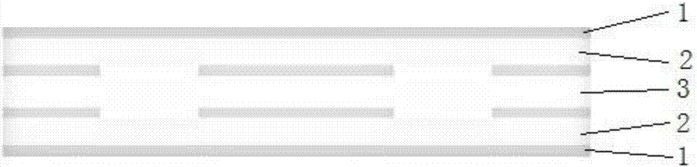
[0028] 1) Lamination is composed of circuit board 1, core board dielectric layer 2, circuit board 1, insulating layer 3, circuit board 1, core board dielectric layer 2 and circuit board 1 to form a PCB board, and the operating parameter is vacuum state The lamination pressure is controlled at 320psi, the circuit board 1 is raised from room temperature to 185°C, the heating rate is controlled at 2.5°C / min in the range of 100°C-170°C, the high temperature is maintained at 185°C for 60min, and then cooled to room temperature , the cooling rate is less than 3°C / min;

[0029] 2) Drilling, drilling in the vertical direction of the PCB board;

[0030] 3) Immerse copper to make the hole wall of the drilled PCB board conductive and form a metallized through hole. The copper thickness obtained by immersion copper plating is 5 μm;

[0031] 4) Solder resist plugging holes, through the solder resist ink 4...

Embodiment 2

[0036] A PCB board processing technology, comprising the following process steps,

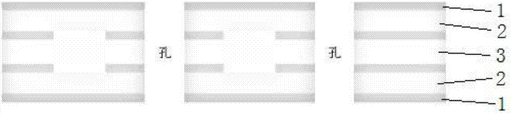
[0037] 1) Lamination is composed of circuit board 1, core board dielectric layer 2, circuit board 1, insulating layer 3, circuit board 1, core board dielectric layer 2 and circuit board 1 to form a PCB board, and the operating parameter is vacuum state The lamination pressure is controlled at 380psi, the circuit board 1 is raised from room temperature to 175°C, the heating rate is controlled at 3.5°C / min in the range of 100°C-170°C, the high temperature is maintained at 175°C for 70min, and then cooled to room temperature , the cooling rate is less than 3°C / min;

[0038] 2) Drilling, drilling in the vertical direction of the PCB board;

[0039] 3) Immerse copper to make the hole wall of the drilled PCB board conductive and form a metallized through hole. The copper thickness obtained by immersion copper plating is 15 μm;

[0040] 4) Solder resist plugging holes, through the solder resist ink ...

Embodiment 3

[0045] A PCB board processing technology, comprising the following process steps,

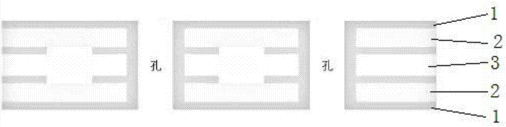
[0046] 1) Lamination is composed of circuit board 1, core board dielectric layer 2, circuit board 1, insulating layer 3, circuit board 1, core board dielectric layer 2 and circuit board 1 to form a PCB board, and the operating parameter is vacuum state The lamination pressure is controlled at 350psi, and the circuit board 1 is raised from room temperature to 180°C, and the heating rate is controlled at 3°C / min in the range of 100°C-170°C, and the high temperature is maintained at 180°C for 65min, and then cooled to room temperature , the cooling rate is less than 3°C / min;

[0047] 2) Drilling, drilling in the vertical direction of the PCB board;

[0048] 3) Immerse copper to make the hole wall of the drilled PCB board conductive and form metallized through holes. The thickness of copper obtained by immersion copper plating is 10 μm;

[0049] 4) Solder resist plugging holes, through the solder...


PUM


Abstract

The invention discloses a machining process of a PCB. The machining process comprises the following steps: laminating, drilling, electrodeless plating copper, resistance-soldering plughole, resistance-soldering baking, ceramic plate grinding, imaging by virtue of external light, resistance-soldering silk printing, and resistance-soldering baking, wherein the resistance-soldering plughole process is advanced to the step subsequent to the electrodeless plating copper from the normal machining step behind the external-light imaging, so that the problems that the resin plughole is high in cost, and the product is scraped when in repairing can be solved.

Description

technical field [0001] The invention relates to the field of PCB board processing, in particular to a PCB board processing technology. Background technique [0002] With the development of science and technology, it is an inevitable trend to continuously optimize processing methods, improve production efficiency and product yield, and at the same time require various manufacturing industries to reduce processing costs. The difference in plugging process of PCB products will have certain differences in product yield and cost. According to the characteristics of PCB products that need to be soldered, most product vias need to be made of plugged holes, and in order to reduce PCB processed products, Many customers will choose impedance plug holes, so for some local welding positions, partial windows or single-sided windows are required, and the welding position is only 5mil away from the via hole (general design requires 12mil), and some via holes and welding due to design space...

Claims


Application Information

Patent Timeline
Patent Type & Authority Applications(China)
IPC IPC(8): H05K3/00H05K3/28H05K3/46
CPCH05K3/0094H05K3/282H05K3/4611H05K2203/143
Inventor 李超谋吴传亮任代学
Owner 珠海杰赛科技有限公司
Why Eureka
Try Eureka