
Method for preparing semiconductor nanocrystals by liquid phase ablation of femtosecond laser microchannel

A technology of femtosecond laser and microfluidic channel, which is applied in the direction of laser welding equipment, nanotechnology, chemical instruments and methods, etc., can solve the problems that nanoparticles are easy to agglomerate, so as to avoid amorphous decomposition products, avoid agglomeration effect, avoid Oxidized effect

Active Publication Date: 2019-04-23
SICHUAN UNIV
View PDF6 Cites 0 Cited by
  • Summary
  • Abstract
  • Description
  • Claims
  • Application Information

AI Technical Summary

Problems solved by technology

However, the existing two types of laser liquid phase ablation methods generally have the problem that the nanoparticles produced by the ablation reaction are easy to agglomerate. In order to reduce the agglomeration effect of the product, the method of adding surfactant to the dispersion in advance is often used. However, due to the ablation effect of the laser, the organic surfactant decomposes to form an amorphous carbon coating and forms a carbon coating on the surface of the nanocrystal, thus greatly affecting the optical properties and surface physical and chemical properties of the obtained nanocrystal. Impact
The current laser liquid phase ablation method cannot solve both the problem of agglomeration of nanocrystals in the continuous preparation process and the problem of surface coatings at the same time.

Method used


Image

  • Method for preparing semiconductor nanocrystals by liquid phase ablation of femtosecond laser microchannel
  • Method for preparing semiconductor nanocrystals by liquid phase ablation of femtosecond laser microchannel
  • Method for preparing semiconductor nanocrystals by liquid phase ablation of femtosecond laser microchannel

Examples


Embodiment 1

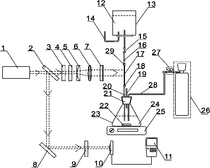
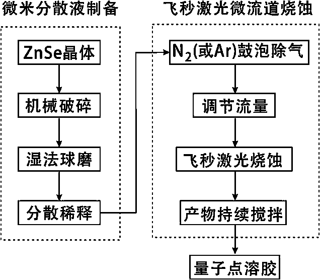
[0036] A method for preparing semiconductor nanocrystals using femtosecond laser microfluidic liquid phase ablation described in this embodiment is as follows: figure 1 The shown device, process steps are as follows:

[0037] (1) Preparation of target material micron particle dispersion

[0038] The zinc selenide polycrystalline block with a purity of 99.99% is first mechanically crushed into particles with a particle size of less than 3 mm, and then an appropriate amount of particles is put into a 100 mL ball mill jar, a small amount of distilled water is added, and the speed is set at about 600 r / min Wet milling is carried out, and the ball milling time is about 6-8 h. After the sample is cooled, wash out the suspension of micron particles obtained after wet grinding, and dilute the suspension for use;

[0039] (2) Construction of microfluidic channel system

[0040] Fill the zinc selenide micron particle distilled water dispersion 12 with a concentration of about 0.5 mg / ...

Embodiment 2

[0046] The method for preparing semiconductor nanocrystals by femtosecond laser microchannel liquid phase ablation described in this example differs from Example 1 in that the target material used in step (1) is chromium-doped zinc selenide (Cr:ZnSe ) crystal; the diameter of the microchannel in step (2) is about 200 μm, and the dispersion liquid used in the collection bottle 23 is distilled water; the single pulse energy of the femtosecond laser in step (3) is about 1.0mJ, and the appearance of the obtained doped nanocrystal is It is a spherical nanoparticle with a particle size of about 10-100 nm. A scanning electron microscope photograph of the product is attached Figure 4 shown.

Embodiment 3

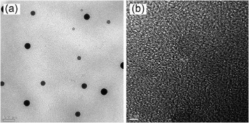
[0048] The method for preparing semiconductor nanocrystals by femtosecond laser microchannel liquid phase ablation described in this example differs from Example 1 in that absolute ethanol is used as the dispersion in step (1); The concentration of zinc selenide microparticles is about 0.25 mg / mL, the dispersion used in the collection bottle 23 is absolute ethanol, and the nitrogen gas cylinder 26 is closed; the single pulse energy in step (3) is 0.8 mJ, and the final product obtained is Zinc selenide nanoparticles coated with a thin layer of amorphous carbon on the surface, spherical in appearance, with a particle size of about 20-100 nm. The transmission electron microscope photograph of its product is attached as Figure 5 As shown in (a), the cladding layer outside the spherical nanocrystals can be seen from the figure. The high-resolution transmission electron microscope photos of the nanocrystals are attached Figure 5 (b) shown.


PUM

PropertyMeasurementUnit
frequencyaaaaaaaaaa
lengthaaaaaaaaaa
sizeaaaaaaaaaa

Abstract

The invention relates to a method for preparing semi-conductor nanocrystallines by femtosecond laser micro-channel liquid phase ablation. The method for preparing the semi-conductor nanocrystalline materials combines the femtosecond laser micro-channel liquid phase ablation technology and the microfluid technology: femtosecond laser is focused in a micro-fluid which flows in a micro-channel and is formed by a doped or intrinsic semiconductor micrometer particle dispersing agent, an ablation reaction region is formed inside the micro-channel, when the dispersing agent loaded with target material micrometer particles passes by the ablation region, ablation reaction occurs in a tiny area in the micro-channel, monodisperse nanocrystallines are formed and flow to a lower part collection device immediately, a pure solvent is used as a dispersion liquid in the collection device, and a nanocrystalline monodisperse liquid product can be obtained; a surfactant solution is used as a dispersion liquid in the collection device, and a nanocrystalline dispersion liquid with a coating can be obtained. According to the method, the technology is simple, the preparation parameters are controllable, no by-product is produced, and the method is an environment-friendly green synthesis technology.

Description

technical field [0001] The invention relates to a method for preparing nanometer materials, in particular to a method for preparing semiconductor nanocrystals by using femtosecond laser microfluidic liquid phase ablation. Background technique [0002] Semiconductor nanocrystals, due to their extremely strong quantum confinement effect, have significantly different energy band structures and band gap sizes from bulk materials, and thus exhibit novel mechanical, optical, electrical and magnetic properties. They are used in optoelectronic devices, Fields such as biomedical markers and solar cells have broad application prospects. As early as 1996, Alivisatos, A. P.[Semiconductor clusters, nanocrystals, and quantum dots[J].Science, 271(5251),933.] research group of the University of California, Berkeley, studied the scale of semiconductor materials from macroscopic solids to nanoscale The change of electronic energy state structure during the transformation process is studied, ...

Claims


Application Information

Patent Timeline
Patent Type & Authority Patents(China)
IPC IPC(8): C01B19/00B82Y40/00B23K26/362B23K26/402
CPCB23K26/361B23K26/402B82Y40/00C01B19/007C01P2002/54C01P2004/03C01P2004/04C01P2004/64
Inventor 冯国英杨超周寿桓
Owner SICHUAN UNIV
Learn More