Chip package and method for forming the same

A technology for a chip package and a manufacturing method, which is applied to the manufacturing of semiconductor/solid-state devices, semiconductor devices, and electric solid-state devices, etc., can solve the problems of reduced quality and reliability of chip packages, reduced thickness and width of wires, and circuit failures. , to achieve the effect of eliminating electromigration phenomenon, improving quality and reliability

Inactive Publication Date: 2017-09-08
XINTEC INC
View PDF4 Cites 5 Cited by
  • Summary
  • Abstract
  • Description
  • Claims
  • Application Information

AI Technical Summary

Problems solved by technology

[0003] However, when the size of the chip package shrinks, the thickness and width of the wires become smaller, and the distance between the wires also becomes narrower, so that circuit failures are prone to occur in the densely populated wiring area.
For example, electromigration and / or Galvanic effect may occur between wires made of metal, which may cause electrical short circuit and / or open circuit, resulting in chip package Body quality and reliability decrease

Method used


Image

  • Chip package and method for forming the same
  • Chip package and method for forming the same
  • Chip package and method for forming the same

Examples


Embodiment Construction

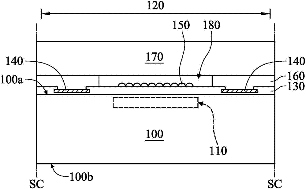
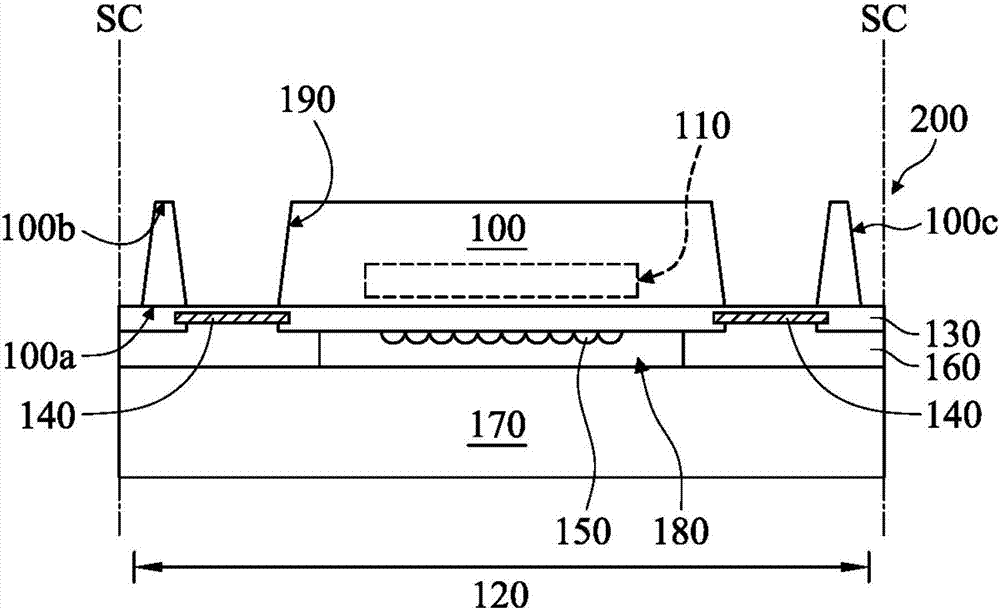
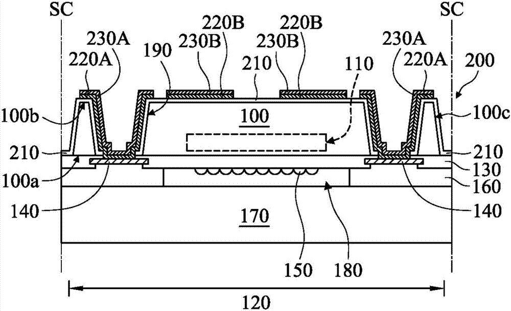
[0014] The fabrication and use of the embodiments of the present invention will be described in detail below. It should be noted, however, that the present invention provides many applicable inventive concepts, which can be embodied in a wide variety of specific forms. The specific embodiments discussed herein are merely specific ways to make and use the invention, and do not limit the scope of the invention. Furthermore, repeated reference numerals or designations may be used in different embodiments. These repetitions are only for the purpose of simply and clearly describing the present invention, and do not represent any relationship between the different embodiments and / or structures discussed. Furthermore, when it is mentioned that a first material layer is located on or above a second material layer, it includes the situation that the first material layer is in direct contact with the second material layer or is separated by one or more other material layers.

[0015] ...


PUM


Abstract

The invention provides a chip package and a method for forming the same. A chip package including a substrate is provided. A sensing region or device region of the substrate is electrically connected to a conducting pad. A first insulating layer is disposed on the substrate. A redistribution layer is disposed on the first insulating layer. A first portion and a second portion of the redistribution layer are electrically connected to the conducting pad. A second insulating layer conformally extends on the first insulating layer, and covers side surfaces of the first portion and the second portion. A protection layer is disposed on the second insulating layer. A portion of the second insulating layer is located between the protection layer and the first insulating layer. The quality and the reliability of the chip package can be greatly improved.

Description

technical field [0001] The present invention relates to a semiconductor packaging technology, in particular to a chip package and a manufacturing method thereof. Background technique [0002] The chip packaging process is an important step in the process of forming electronic products. In addition to protecting the chip therein from external environment pollution, the chip package also provides an electrical connection path between the electronic components inside the chip and the outside world. For example, there are wires in the chip package to form a conductive path. As electronic products gradually develop toward miniaturization, the size of chip packages is also gradually reduced. [0003] However, when the size of the chip package shrinks, the thickness and width of the wires become smaller, and the distance between the wires also becomes narrower, so that circuit faults are likely to occur in the densely populated circuit area. For example, electromigration and / or G...

Claims


Application Information

Patent Timeline
Patent Type & Authority Applications(China)
IPC IPC(8): H01L27/146
CPCH01L27/14632H01L27/14636H01L27/14687H01L23/3114H01L21/561H01L2224/11H01L21/76898H01L24/02H01L24/03H01L24/11H01L24/13H01L2224/0235H01L2224/02372H01L2224/02377H01L2224/02331H01L2224/05582H01L2224/05569H01L2224/0231H01L2224/0239H01L2224/03462H01L2224/03464H01L2224/05008H01L2224/05111H01L2224/05124H01L2224/05147H01L2224/05155H01L2224/05166H01L2224/05169H01L2224/05548H01L2224/05611H01L2224/05624H01L2224/05644H01L2224/05655H01L2224/05666H01L2224/05669H01L2224/1132H01L2224/11462H01L2224/13211H01L2224/0529H01L2224/13247H01L2224/13216H01L2224/13244H01L2224/13255H01L24/05H01L27/14618H01L27/14621H01L27/14627H01L27/14683H01L2924/00014H01L2924/013H01L2924/06H01L2924/01074H01L21/4853H01L21/486H01L23/3171H01L23/5384H01L23/5389H01L2924/146H01L2924/19102H01L2924/301
Inventor 林佳升赖炯霖陈瑰玮
Owner XINTEC INC
Why Eureka
Try Eureka