Array substrate, manufacturing method therefor, and display device
A technology for array substrates and manufacturing methods, which is applied in the direction of electrical components, electrical solid devices, circuits, etc., can solve problems such as thinning and sagging of adhesive materials, disconnection, deformation and expansion of adhesive layers, etc., to achieve large contact area and improve support performance, improve the effect of pressure resistance
- Summary
- Abstract
- Description
- Claims
- Application Information
AI Technical Summary
Problems solved by technology
Method used
Image

Examples
Embodiment Construction
[0041] The present invention will be further described below with reference to the accompanying drawings and exemplary embodiments, wherein the same reference numerals in the accompanying drawings all refer to the same components. Also, detailed descriptions of known arts will be omitted if they are unnecessary to illustrate the features of the present invention.
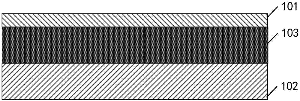
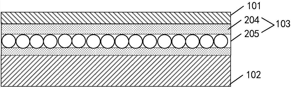
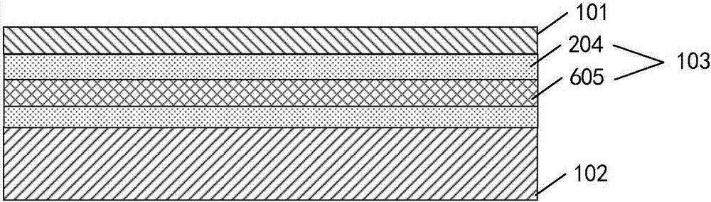
[0042] The structural diagram of the array substrate of the present invention is shown in Figure 1. The array substrate includes a flexible substrate 101, a back protection film 102 and an adhesive layer 103, and the back protection film is connected to the adhesive layer through the adhesive layer. The flexible base substrate is bonded together, and the bonding layer includes glue material and several nano fillers filled in the glue material.
[0043] Wherein, the flexible substrate is preferably a plastic substrate. Compared with the existing glass substrate, the plastic substrate has better flexibility, is less ...
PUM
 Abstract
Description
Claims
Application Information
 - R&D
- Intellectual Property
- Life Sciences
- Materials
- Tech Scout
- Unparalleled Data Quality
- Higher Quality Content
- 60% Fewer Hallucinations
Browse by: Latest US Patents, China's latest patents, Technical Efficacy Thesaurus, Application Domain, Technology Topic, Popular Technical Reports.
© 2025 PatSnap. All rights reserved.Legal|Privacy policy|Modern Slavery Act Transparency Statement|Sitemap|About US| Contact US: help@patsnap.com