PCB (Printed Circuit Board) placing box

A PCB board and storage box technology, applied in the field of electronic information, can solve problems such as poor practicability, dirty PCB boards, and accumulated dust, and achieve the effects of high work efficiency, simple and fast operation, and simple structure

Active Publication Date: 2017-09-22
NANTONG DUOQIAN NEW MATERIAL SCI & TECH CO LTD
View PDF6 Cites 0 Cited by
  • Summary
  • Abstract
  • Description
  • Claims
  • Application Information

AI Technical Summary

Problems solved by technology

In the PCB production process, the PCB board needs to be temporarily stored on the rack between each process. The existing open rack is easy to accumulate dust during actual operation, resulting in the PCB board being dirty, and the positioning, picking and placing of the carrier board is difficult. The handling operation is cumbersome and the practicability is poor

Method used


Image

  • PCB (Printed Circuit Board) placing box
  • PCB (Printed Circuit Board) placing box

Examples


Embodiment Construction

[0016] In order to deepen the understanding of the present invention, the present invention will be further described below in conjunction with the embodiments and accompanying drawings. The embodiments are only used to explain the present invention and do not constitute a limitation to the protection scope of the present invention.

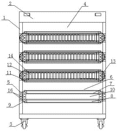
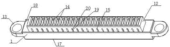
[0017] Such as figure 1 and figure 2 A PCB board placement box is shown, including a box body 1, an accommodating cavity 4, a connecting seat 5, a bracket body 6 and a carrier board assembly, the top of the box body 1 is a loading platform 2, and the bottom of the box body 1 is set There are universal wheels 2, and a housing cavity 4 is arranged in the box body 1. At least one set of connection seats 5 are arranged symmetrically on the side walls of the accommodation cavity 4, and at least one bracket body 6 is arranged between at least one group of connection seats 5. , at least one bracket body 6 includes a bracket body I7 and a bracket body ...


PUM


Abstract

The invention discloses a PCB (Printed Circuit Board) placing box. The PCB placing box comprises a box body, a containing cavity, connecting seats, bracket bodies and support plate assemblies, wherein the containing cavity is formed in the box body, at least one group of connecting seats are symmetrically arranged on the side wall of the containing cavity, at least one bracket body is arranged between the at least one group of connecting seats and includes a bracket monomer I and a bracket monomer II, the single support plate assembly comprises a base and a support plate, positioning parts are arranged on both ends of the base, the support plate is arranged on the upper end surface of the base in a sliding mode, and a plurality of slots which are matched with products are formed in the support plate. The PCB placing box has the advantages of simple structure, good universality, convenience, practicability, simplicity and rapidity in operation and high working efficiency, a plurality of support plate assemblies are arranged in the box body through brackets and the connecting seats so as to form a closed structure, the condition of accumulating dust, dirt and the like is effectively avoided when a PCB is placed, independent use, maintenance or replacement can be realized, and the PCB can be positioned only by pulling a positioning block.

Description

technical field [0001] The invention relates to the technical field of electronic information, in particular to a PCB board placement box. Background technique [0002] PCB board is an important electronic component, a support for electronic components, and a carrier for electrical connections of electronic components. Printed boards have developed from single-layer to double-sided, multi-layer and flexible, and still maintain their respective development trend. In the PCB production process, the PCB board needs to be temporarily stored on the rack between each process. The existing open rack is easy to accumulate dust during actual operation, resulting in the PCB board being dirty, and the positioning, picking and placing of the carrier board is difficult. The handling operation is comparatively loaded down with trivial details, practicality is relatively poor. [0003] Therefore, in order to solve the above-mentioned existing problems, the present invention provides a ne...

Claims


Application Information

Patent Timeline
Patent Type & Authority Applications(China)
IPC IPC(8): B65D25/24B65D25/02B65D25/10B65D85/86
CPCB65D25/02B65D25/10B65D25/24H05K13/0061
Inventor 王端广
Owner NANTONG DUOQIAN NEW MATERIAL SCI & TECH CO LTD
Why Eureka
Try Eureka