Method for manufacturing semiconductor device, and semiconductor device

A manufacturing method and semiconductor technology, applied in the direction of semiconductor/solid-state device manufacturing, semiconductor devices, semiconductor/solid-state device components, etc., can solve problems such as poor connection and achieve the effect of suppressing position shift

Active Publication Date: 2017-09-26
株式会社PANGEA
View PDF5 Cites 7 Cited by
  • Summary
  • Abstract
  • Description
  • Claims
  • Application Information

AI Technical Summary

Problems solved by technology

If positional deviation occurs, there may be poor connection between the external connection terminal and the circuit board

Method used


Image

  • Method for manufacturing semiconductor device, and semiconductor device
  • Method for manufacturing semiconductor device, and semiconductor device
  • Method for manufacturing semiconductor device, and semiconductor device

Examples


Embodiment Construction

[0018] Embodiments will be described below with reference to the drawings. In addition, the drawings are schematic diagrams, and for example, the relationship between the thickness and the plane size, the ratio of the thickness of each layer, and the like may be different from the actual ones. In addition, in the embodiments, substantially the same components are given the same reference numerals and descriptions thereof are omitted.

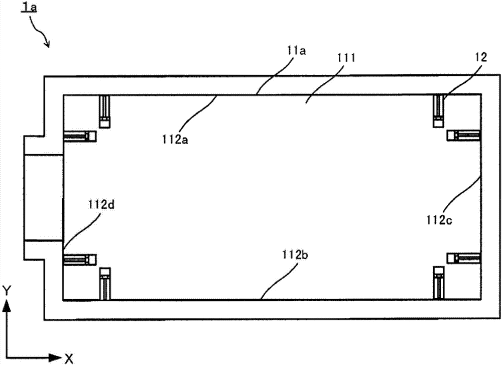
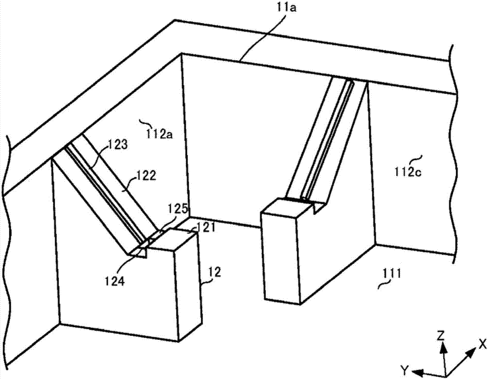
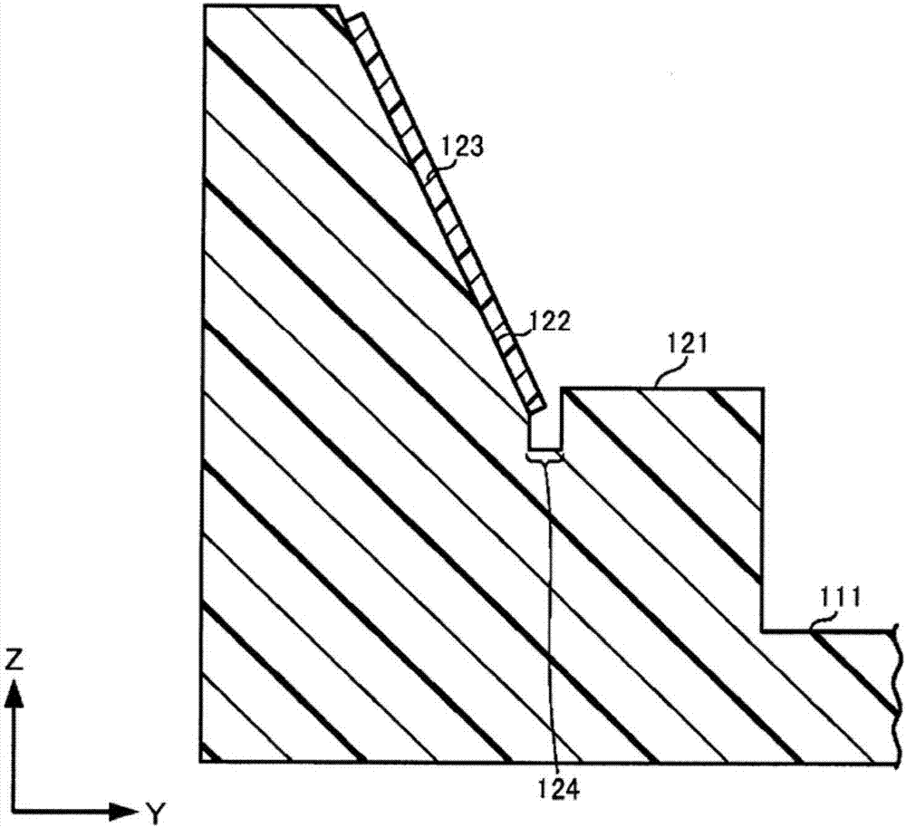
[0019] As an example of the manufacturing method of the semiconductor device of this embodiment, refer to Figure 1 to Figure 8 An example of a method of manufacturing a semiconductor device capable of data transmission using a USB (Universal Serial Bus: Universal Serial Bus) by connecting to a socket will be described. In addition, the present invention is not limited thereto, and may be a semiconductor device capable of data transfer by methods other than USB.

[0020] An example of a method for manufacturing a semiconductor device includes:...


PUM


Abstract

The embodiment of the invention provides a manufacturing method and a semiconductor device of a semiconductor device capable of suppressing a positional deviation of a circuit board. The method for manufacturing a semiconductor device according to the embodiment includes the steps of holding a part of the pressing rib while flattening the circuit board from the side facing the bottom surface while maintaining the circuit board toward the first surface, and the first case And a substrate holding rib having a first surface, a second surface, an extrusion rib, and a groove, and the first surface is positioned on the first and second surfaces of the first recess, and the second surface is inclined from the wall surface of the first recess to the bottom surface of the first recess, and the pressing rib extends in the oblique direction of the second surface so as to protrude from the second surface, and the groove is provided between the first surface and the second surface so as to be in contact with the lower end of the second surface.

Description

[0001] [Related Application] [0002] This application enjoys the priority of the basic application based on Japanese Patent Application No. 2016-53149 (filing date: March 16, 2016). This application incorporates the entire content of the basic application by referring to this basic application. technical field [0003] Embodiments relate to a method of manufacturing a semiconductor device and the semiconductor device. Background technique [0004] A semiconductor device such as a memory capable of data transmission is formed by holding a circuit board having a semiconductor chip in a case and electrically connecting external connection terminals to the circuit board. [0005] The size of the case used in the semiconductor device and the size of the circuit board tend to vary during the manufacturing steps. If the deviation occurs, there is a case where the position of the circuit board is shifted when the circuit board is held in the housing. If positional deviation occu...

Claims


Application Information

Patent Timeline
Patent Type & Authority Applications(China)
IPC IPC(8): H01L21/52H01L23/10
CPCH01L21/52H01L23/10
Inventor 三野利一
Owner 株式会社PANGEA
Why Eureka
Try Eureka