Integrated semiconductor bridge transduction element

A technology of transducing components and semiconductors, which is applied in the direction of weapon accessories, blasting barrels, offensive equipment, etc., can solve problems such as interference, electromagnetic damage, and heat accumulation damage of electrical explosives, and achieve strong anti-electromagnetic interference performance and large design margin , the effect of improving reliability

Active Publication Date: 2017-09-29
司马博羽
View PDF8 Cites 4 Cited by
  • Summary
  • Abstract
  • Description
  • Claims
  • Application Information

AI Technical Summary

Problems solved by technology

However, this technical solution cannot solve other forms of electromagnetic interference problems at the same time, such as electromagnetic radiation and stray current interference, which will cause damage caused by the heat accumulation of electrical explosives
[0005] In short, the existing technical solutions can only achieve a strengthening effect on a certain damage of the electromagnetic field, and only improve the safety of semiconductor bridge pyrotechnics from a certain aspect, and cannot take into account the reliability of ignition while improving safety.
For example, the above-mentioned technical solutions either only improve the anti-static ability, or only improve the anti-interference ability to electromagnetic radiation or stray current, and cannot comprehensively solve all electromagnetic damage problems through a technical solution
In addition, the ignition reliability performance of the existing technical solutions is also insufficient. The traditional semiconductor bridge has only one bridge area, and the conversion utilization rate of the input energy is low. Only a single bridge area can be converted to form a limited plasma effect, which cannot be reliably ignited. Insensitive Pyrotechnic Potion

Method used


Image

  • Integrated semiconductor bridge transduction element
  • Integrated semiconductor bridge transduction element
  • Integrated semiconductor bridge transduction element

Examples


Embodiment

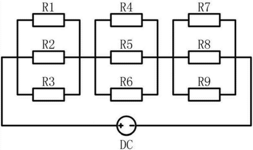
[0059] figure 1 It is the schematic diagram of the series-parallel circuit of the integrated semiconductor bridge. The integrated semiconductor bridge is designed according to the safety and reliability requirements of the ignition system. Parallel and series-parallel hybrid circuits,

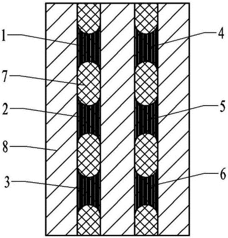
[0060] combine figure 2 1, 2, 3, 4, 5 and 6 in the figure are respectively series-parallel semiconductor bridges formed by six semiconductor bridge regions, each having a different position, 7 is an electrode layer, and 8 is an insulating layer. The reinforcement of the electromagnetic environment interference energy is shared by the six bridges. When the ignition input energy is applied, the six bridges respectively convert and output six plasmas to ignite the pyrotechnic agent at their respective positions.

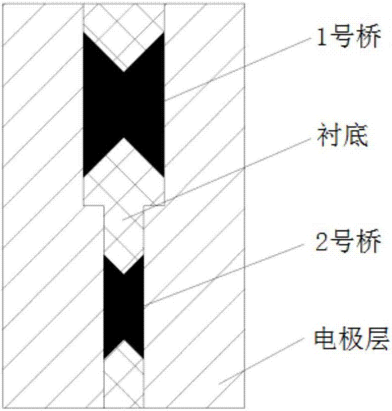
[0061] combine image 3 with Figure 4 , In the high insensitivity pyrotechnics integrated parallel semiconductor bridge, N bridges are formed into a parallel circuit, and the two b...


PUM


Abstract

The invention provides an integrated semiconductor bridge transduction element. The integrated semiconductor bridge transduction element comprises more than two semiconductor bridges, wherein at least one semiconductor bridge is used for absorbing electromagnetic interference energy, and other semiconductor bridges are used for converting input energy into plasma ignition energy; a resistance value, a bridge area and a bridge shape of at least one semiconductor bridge are different from that of other semiconductor bridges; resistance values, bridge areas or bridge shapes of all semiconductor bridges are determined according to ignition positions and timing sequence; all of the semiconductor bridges are connected in series or in parallel or are in series-parallel connection, and the resistance values, the bridge areas or the bridge shapes of all of the semiconductor bridges can be determined according to the ignition positions and the timing sequence; and open circuit resistors are integrated in the bridge areas or electrode areas. According to the integrated semiconductor bridge transduction element, the safety and the reliability are increased, and multi-point sequential ignition can be realized.

Description

technical field [0001] The invention belongs to the technical field of semiconductor bridge pyrotechnics, and in particular relates to an integrated semiconductor bridge transducing element. Background technique [0002] Semiconductor bridge pyrotechnic products are widely used in ignition and detonation systems of weapon systems and civilian blasting equipment due to their excellent quality. At the same time, with the increasingly harsh electromagnetic environment, the requirements for the anti-electromagnetic environment capability of semiconductor bridge pyrotechnic products are also getting higher and higher. For example, for its safety, it is generally required to achieve 1.A.1W.5min insensitivity or higher insensitivity, and for its reliability, its reliability is generally required to be 0.995-0.9999 (confidence level 0.95). Existing semiconductor bridge chips have been difficult to resist external electromagnetic field energy interference in harsh electromagnetic en...

Claims


Application Information

Patent Timeline
Patent Type & Authority Applications(China)
IPC IPC(8): F42B3/13
CPCF42B3/13
Inventor 司马博羽
Owner 司马博羽
Why Eureka
Try Eureka