Differential via hole pair inspection tool for PCB

A technology of differential vias and detection tools, which is applied in special data processing applications, instruments, and electrical digital data processing, etc. The effect of missing detection and high accuracy

Inactive Publication Date: 2017-09-29
ZHENGZHOU YUNHAI INFORMATION TECH CO LTD
View PDF7 Cites 13 Cited by
  • Summary
  • Abstract
  • Description
  • Claims
  • Application Information

AI Technical Summary

Problems solved by technology

The current inspection method is manual, that is, it is necessary to manually check the size of each pair of differential vias one by one, which is not only time-consuming and laborious, but also has low detection accuracy and is prone to missed inspections.

Method used


Image

  • Differential via hole pair inspection tool for PCB
  • Differential via hole pair inspection tool for PCB

Examples


Embodiment Construction

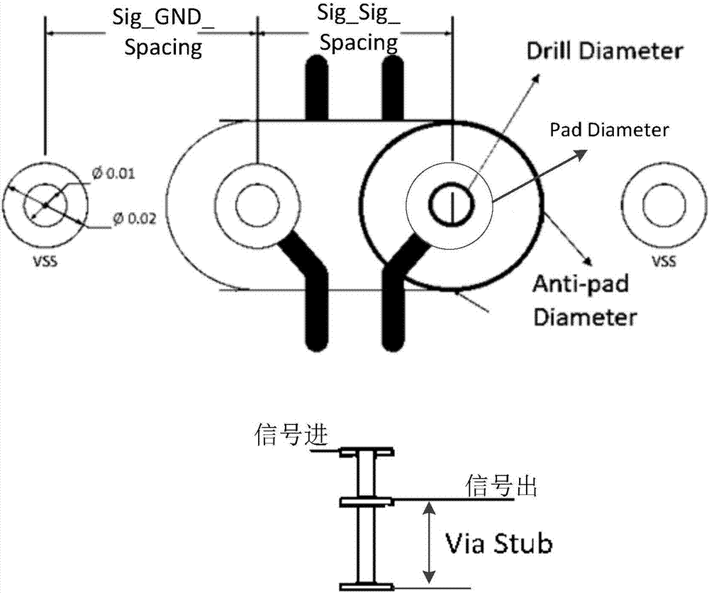
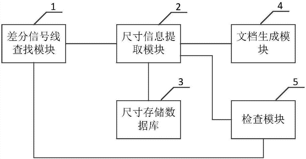
[0028] The core of the invention is to provide a differential via pair detection tool for PCB, which can automatically complete the search of several pairs of differential signal lines and the acquisition of the size information of the corresponding differential via pair, saves manpower, and has a fast detection speed. The accuracy is high, and missed detection is avoided as much as possible.

[0029] In order to make the purposes, technical solutions and advantages of the embodiments of the present invention clearer, the technical solutions in the embodiments of the present invention will be clearly and completely described below with reference to the accompanying drawings in the embodiments of the present invention. Obviously, the described embodiments These are some embodiments of the present invention, but not all embodiments. Based on the embodiments of the present invention, all other embodiments obtained by those of ordinary skill in the art without creative efforts sha...


PUM


Abstract

The invention discloses a differential via hole pair inspection tool for a PCB. The tool comprises a differential signal line search module, a dimension information extraction module, and a dimension storage database, wherein the differential signal line search module is used for receiving identifiers of to-be-inspected differential signal lines inputted by a user; the to-be-inspected differential signal lines are obtained by searching from a preset routing database according to the identifiers, the dimension information extraction module is used for obtaining the dimension information of a pair of differential via holes corresponding to each pair of to-be-inspected differential signal lines by extracting from a PCB board through calculation, the dimension storage database is used for storing the dimension information for subsequent via hole inspection. The differential via hole pair inspection tool for PCB is capable of automatically completing the search of pairs of differential signal lines and acquiring the dimension information of the corresponding differential via hole pairs, and has the advantages of being manpower-saving, high in inspection speed, and high in accuracy, and the situation of missing inspection is avoided as far as possible.

Description

technical field [0001] The invention relates to the technical field of circuit wiring detection, in particular to a differential via pair detection tool for PCB. Background technique [0002] In cloud computing products (servers, storage, etc.), the transmission rate of signal lines on boards such as motherboards and high-speed backplanes is getting faster and faster, and the requirements for signal impedance continuity are getting higher and higher. Since the transmission line encounters the via hole, the impedance will be reduced, so the impedance of the transmission line and the via hole will be discontinuous, resulting in SI (Signal Integrity, signal integrity) problems such as reflection. In order to maintain the continuity of signal impedance, SI engineers will optimize the impedance of the vias and provide the layout engineers with the dimensions of the differential vias. [0003] In order to ensure that the wiring is set according to this size specification, after t...

Claims


Application Information

Patent Timeline
Patent Type & Authority Applications(China)
IPC IPC(8): G06F17/50
CPCG06F30/398
Inventor 李艳军
Owner ZHENGZHOU YUNHAI INFORMATION TECH CO LTD
Why Eureka
Try Eureka