PCB (printed circuit board) defect mass detection system and method

A PCB circuit board, batch detection technology, applied in the field of detection system, to achieve the effect of saving manpower and time, good directivity, and a wide range of fault detection

Active Publication Date: 2013-11-20
中科芯未来微电子科技成都有限公司
View PDF3 Cites 50 Cited by
  • Summary
  • Abstract
  • Description
  • Claims
  • Application Information

AI Technical Summary

Problems solved by technology

[0006] The purpose of the present invention is to overcome the deficiencies in the prior art, and provide a PCB circuit board defect batch detection system and related detection methods. Detect a variety of circuit faults, including circuit

Method used


Image

  • PCB (printed circuit board) defect mass detection system and method
  • PCB (printed circuit board) defect mass detection system and method
  • PCB (printed circuit board) defect mass detection system and method

Examples


Example Embodiment

[0043] The present invention will be further described below with reference to the specific drawings and embodiments.

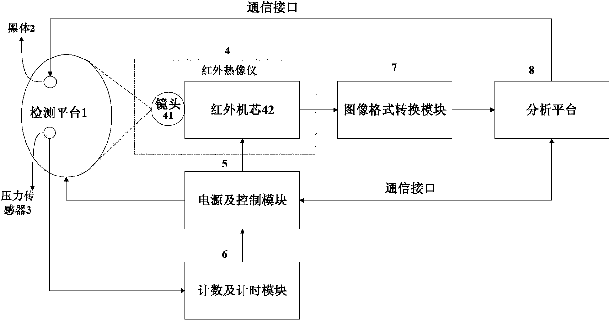
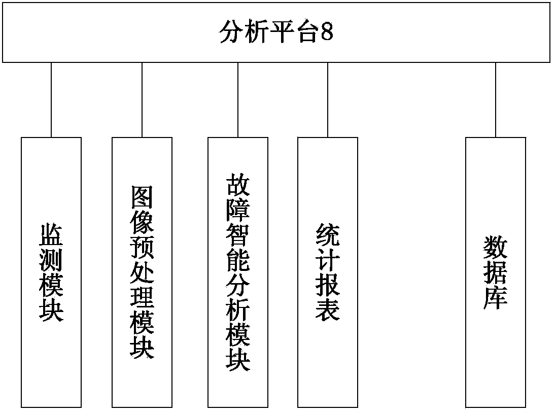
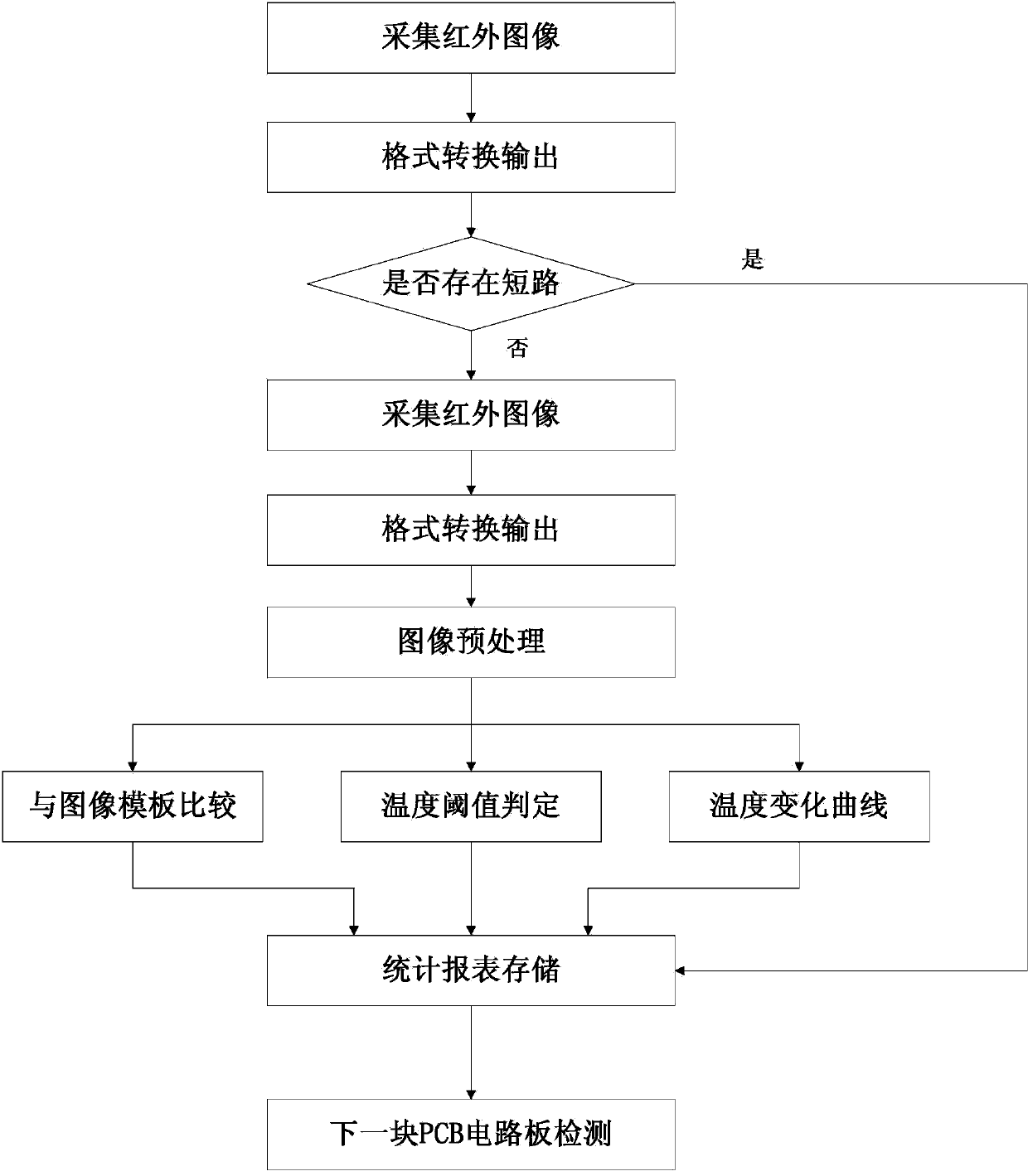
[0044] like figure 1 As shown, a batch detection system for PCB circuit board defects includes:

[0045]The infrared thermal imager 4 includes an infrared lens 41 and an infrared core 42. The infrared radiation energy of the detected PCB circuit board is collected by the infrared lens 41, and the optical path adjustment is sensed by the sensor of the infrared core 42, and the infrared core 42 converts the light signal. into electrical signals and output infrared images in analog video format;

[0046] The black body 2 is set on the detection platform 1 to provide a reference for the target temperature measurement. The PC can set the radiation temperature of its temperature cooling surface through the communication interface, and its temperature cooling surface is set in the imaging field of the infrared thermal imager 4; PCB circuit The temperature under th...


PUM


Abstract

The invention provides a PCB (printed circuit board) defect mass detection system, which comprises a thermal infrared imager, a black body, a detection platform, a pressure sensor, an image format conversion module, a power supply and control module, a counting and timing module and an analysis platform, wherein the thermal infrared imager collects the infrared radiation energy of a detected PCB and outputs corresponding infrared images, the black body provides reference for the target temperature measurement, the power supply and control module provides excitation signals of the detected PCB, and controls the work of the thermal infrared imager, the counting and timing module carries out counting coding on the detected PCB and records the excitation signal duration of the detected PCB, the analysis platform analyzes and processes the temperature information and infrared images of the detected PCB in the electrified stage, the fault information of the detected PCB is obtained, and a statistical form is produced. The PCB defect mass detection system has the advantages that the infrared images of the tested PCB in the electrified state are obtained, various kinds of circuit faults can be automatically detected, the detection fault range is wide, and the fully automatic fast and continuous detection is realized.

Description

technical field [0001] The invention relates to a detection system, in particular to a system and method for batch detection of PCB circuit board defects. Background technique [0002] Almost all integrated circuit-based electronic devices use printed circuit boards (PCBs) for electrical interconnection between electronic components. When mass-producing electronic equipment, it is necessary to solder a large number of components on the printed circuit board, and there are often circuit faults, including circuit faults such as short circuits, open circuits and poor contact, and device faults caused by component quality problems, which need to undergo rigorous testing. Make sure that there is no circuit failure before it can be put on the market. [0003] Conventional circuit fault detection mainly measures the necessary parameters of key points and lines in the circuit, including voltage, current, impedance and components, etc., and carefully analyzes the circuit principle i...

Claims


Application Information

Patent Timeline
IPC IPC(8): G01R31/02G01N25/72
Inventor 代旭东陈小翔张雷
Owner 中科芯未来微电子科技成都有限公司
Why Eureka
Try Eureka