Nanowire array preparation method, nanowire array integrated device and preparation method thereof

A nanowire array and integrated device technology, which is applied in semiconductor/solid-state device manufacturing, nanotechnology, semiconductor devices, etc., can solve the problems of cumbersome steps, lower yield, and uncontrollability, so as to simplify the manufacturing process and improve yield , the effect of improving controllability

Inactive Publication Date: 2016-11-09
SOUTH CHINA NORMAL UNIVERSITY
View PDF5 Cites 15 Cited by
  • Summary
  • Abstract
  • Description
  • Claims
  • Application Information

AI Technical Summary

Problems solved by technology

[0005] However, at present, the orderly growth of high-quality nanowire arrays is still immature, and the operation is difficult, uncontrollable, and the success rate is low, which severely limits the excellent performance of nanowire devices.
Existing nanowire devices are transferred to new substrates by stripping, and the arrangement has uneven distribution, disorder, and randomness, which greatly reduces the yield, thus affecting the testing and performance research of nanowire devices.
Moreover, the design process of nanowire array devices is complex and the steps are cumbersome, which brings difficulties to device preparation.

Method used


Image

  • Nanowire array preparation method, nanowire array integrated device and preparation method thereof
  • Nanowire array preparation method, nanowire array integrated device and preparation method thereof
  • Nanowire array preparation method, nanowire array integrated device and preparation method thereof

Examples


Embodiment 1

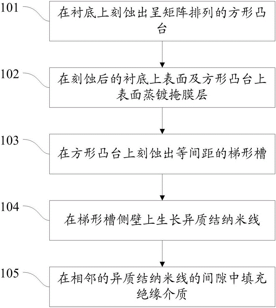
[0062] figure 1 An overall flowchart of a method for preparing a nanowire array provided by the present invention; as figure 1 As shown, a method for preparing a nanowire array provided by the present invention includes:

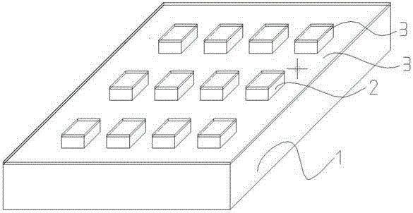
[0063] Step 101: etching square bosses arranged in a matrix on the substrate; the substrate is a single crystal silicon substrate;

[0064] Step 102: evaporating a mask layer on the etched upper surface of the substrate and the upper surface of the square boss; the mask layer is a silicon dioxide layer with a thickness of 100-200 nm;

[0065] Step 103: Etching equidistant trapezoidal grooves on the square boss;

[0066] Step 104: growing heterojunction nanowires on the sidewalls of the trapezoidal groove;

[0067] Specifically, first put the substrate with etched trapezoidal groove into the reaction chamber of metal organic chemical vapor deposition system, and grow an AlN buffer layer on the side wall of the trapezoidal groove to reduce the stress of the...

Embodiment 2

[0093] Embodiment 2: combined reference Figure 5-9 , using photoresist as a mask, combining photolithography technology and ICP technology to prepare a square boss 2, the height of the square boss 2 is 4-8um.

[0094] Evaporate a silicon dioxide mask layer 3 with a thickness of 100 to 200 nm on the surface of the substrate 1, use acetone and isopropanol to ultrasonically clean and dry the surface of the silicon dioxide mask layer 3, and spin coat on the mask layer 3 Photoresist positive resist; then use a set spacing equal-spaced stripe photolithography plate for exposure, the stripe spacing is 3-6um; then develop, remove the exposed photoresist positive resist, and the remaining photoresist forms a stripe pattern; use BOE The silicon dioxide mask layer 3 not covered by the photoresist is etched with a solution, and the etching depth is exactly 100-200 nm in thickness of the mask layer 3; then the KOH solution wet-etches the part not covered by the mask layer 3, and the etche...

Embodiment 3

[0098] Embodiment 3, in conjunction with reference Figure 5-9 , using photoresist as a mask, combining photolithography technology and ICP technology to prepare a square boss 2, the height of the square boss 2 is 4-8um.

[0099] Evaporate a silicon dioxide mask layer 3 with a thickness of 100 to 200 nm on the surface of the substrate 1, use acetone and isopropanol to ultrasonically clean and dry the surface of the silicon dioxide mask layer 3, and spin coat on the mask layer 3 Photoresist positive resist; then use a set spacing equal-spaced stripe photolithography plate for exposure, the stripe spacing is 3-6um; then develop, remove the exposed photoresist positive resist, and the remaining photoresist forms a stripe pattern; use BOE The silicon dioxide mask layer 3 not covered by the photoresist is etched with a solution, and the etching depth is exactly 100-200 nm in thickness of the mask layer 3; then the KOH solution wet-etches the part not covered by the mask layer 3, an...


PUM

PropertyMeasurementUnit
thicknessaaaaaaaaaa

Abstract

The invention discloses a nanowire array preparation method, a nanowire array integrated device and a preparation method thereof. The nanowire array preparation method includes the steps that square bosses which are arranged in a matrix mode are etched on a substrate; mask layers are arranged on the upper surface of the etched substrate and the upper surfaces of the square bosses in an evaporation plating mode; trapezoid grooves are etched in the square bosses at equal intervals; heterostructure nanowires are grown on the side walls of the trapezoid grooves; each gap between every two adjacent heterostructure nanowires is filled with an insulating medium. The nanowire array and the nanowire array integrated device prepared through the method can grow in batches, and directionality and the ordering property are achieved; a grown micro-nano material has controllability.

Description

technical field [0001] The invention relates to the technical field of semiconductor nano devices, in particular to a method for preparing a nanowire array, a nanowire array integrated device and a preparation method thereof. Background technique [0002] The so-called nanoarray refers to one-dimensional nanomaterials such as nanowires, nanorods, and nanotubes, or two-dimensional nanostructures such as nanosheets and nanobelts, and three-dimensional nanostructures such as nanoflowers and nanotrees that are ordered within a certain space. Arrange the array formed. They have more outstanding properties such as surface effects and quantum effects than disordered nanomaterials. By controlling the arrangement of the nanostructure units in the array, nanostructures with specific shapes and sizes can be assembled to achieve improvements in their optical, electrical, and magnetic properties. Therefore, the preparation of highly ordered nano-arrays is of great significance for stud...

Claims


Application Information

Patent Timeline
Patent Type & Authority Applications(China)
IPC IPC(8): B82Y40/00H01L21/3065H01L29/778H01L21/77
CPCB82Y40/00H01L21/3065H01L29/66462H01L29/778
Inventor 李述体王汝鹏宋伟东郭德霄陈航李凯
Owner SOUTH CHINA NORMAL UNIVERSITY
Why Eureka
Try Eureka