Deep submicron CMOS bootstrap switch of eliminating substrate bias effect
A bootstrap switch, deep sub-micron technology, used in electronic switches, analog-to-digital converters, electrical components, etc., can solve problems such as poor linearity, achieve good linearity, eliminate offset effect, and high reliability. Effect
- Summary
- Abstract
- Description
- Claims
- Application Information
AI Technical Summary
Problems solved by technology
Method used
Image

Examples
Embodiment Construction
[0022] The preferred embodiments of the present invention will be described in detail below in conjunction with the accompanying drawings; it should be understood that the preferred embodiments are only for illustrating the present invention, rather than limiting the protection scope of the present invention.
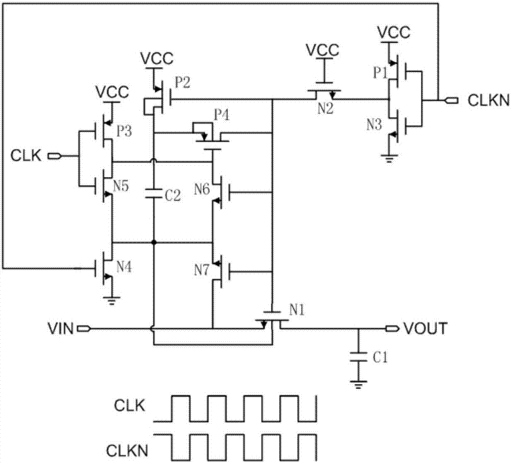
[0023] Such as figure 2 As shown, the clock signals CLK and CLKN are a pair of clock signals that are opposite to each other. In the holding phase, when the clock signal CLK is at low level, CLKN is at high level, NMOS transistor N3 is turned on, PMOS transistor P1 is turned off, the gate of NMOS transistor N1 is connected to the ground through NMOS transistor N2, NMOS transistor N1 is turned off, and the input The signal VIN is disconnected from the sampling capacitor C1, and the signal is held on the sampling capacitor.
[0024] In the holding phase, the gate of the PMOS transistor P2 is connected to the ground through the transistor N2, the transistor P2 is turned ...
PUM
 Abstract
Description
Claims
Application Information