

Semiconductor device and access management method
An access management, semiconductor technology used in the field of controlling access to shared resources to ensure exclusivity
- Summary
- Abstract
- Description
- Claims
- Application Information
AI Technical Summary
Problems solved by technology
Method used
Image

Examples
no. 1 example
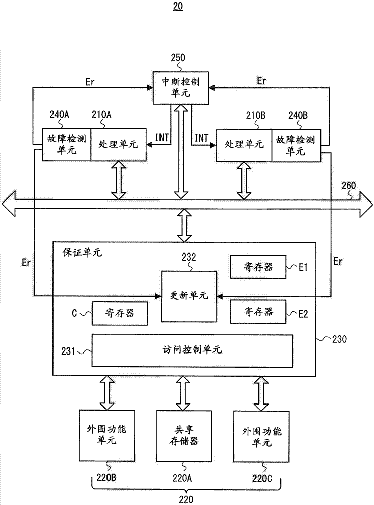
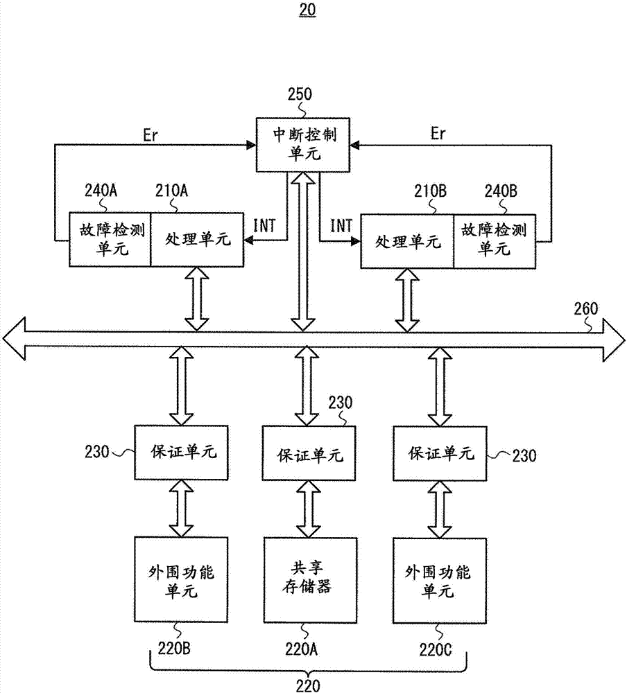
[0033] Next, details of an embodiment are explained. figure 2 is a block diagram showing a simplified configuration example of the semiconductor device 20 according to the first embodiment. Such as figure 2 As shown, semiconductor device 20 includes processing units 210A and 210B, shared memory 220A, peripheral function units 220B and 220C, assurance unit 230 , failure detection units 240A and 240B, and interrupt control unit 250 . It should be noted that two processing units are shown as figure 2 processing unit in . However, the number of processing units is not limited to two as long as the semiconductor device 20 includes at least two processing units. It should be noted that in the following description, the plurality of processing units 210A and 210B may be simply referred to as "processing unit 210" when there is no need to distinguish them from each other. Also, the plurality of failure detection units 240A and 240B may be simply referred to as "failure detectio...
no. 2 example
[0083] Next, a second embodiment is explained. Differences from the first embodiment are explained in detail below, and explanations of configurations and operations similar to those of the first embodiment are omitted. In the semiconductor device 20 according to the first embodiment, when a failure occurs in the processing unit 210, the update unit 232 of the guarantee unit 230 changes the access control so that another processing unit 210 which takes over the processing of the failed processing unit 210 can access Access destinations required to process transfers.
[0084] In contrast, when a failure occurs in the processing unit 210, the semiconductor device 20 according to this embodiment not only changes the access control as described in the first embodiment above, but also changes the access control so that the predetermined processing unit 210 is prohibited from accessing intended destination of visit. Specifically, for example, when the processing unit 210 fails, in...
no. 3 example
[0107] In the above-described embodiment, when a failure in the processing unit 210 is detected only once, the access control is changed. Unlike this, in this embodiment, access control is changed when failures in the same processing unit 210 are detected more than a predetermined number of times. Figure 8 is a block diagram showing a simplified configuration example of the semiconductor device 30 according to the third embodiment. Such as Figure 8As shown, the semiconductor device 30 differs from the semiconductor device 20 in that the semiconductor device 30 includes retry units 300A and 300B. Regarding the configuration and operation of the semiconductor device 30 , only differences from the semiconductor device 20 are explained in detail below, and explanations of similar configurations and operations to the semiconductor device 20 are appropriately omitted. It should be noted that in the following description, the plurality of retry units 300A and 300B may be simply r...
PUM
 Abstract
Description
Claims
Application Information