Check patentability & draft patents in minutes with Patsnap Eureka AI!

Pixel structure

A technology of pixel structure and pixel area, applied in electrical components, electric solid-state devices, circuits, etc., can solve the design problems affecting the resolution of RGB sub-pixel panels, reduce production costs and process difficulties, improve applicability, reduce The effect of the number of uses

Active Publication Date: 2017-10-27
AU OPTRONICS CORP
View PDF4 Cites 1 Cited by
  • Summary
  • Abstract
  • Description
  • Claims
  • Application Information

AI Technical Summary

Problems solved by technology

These technical bottlenecks directly affect the spacing between RGB sub-pixels and the design of panel resolution

Method used


Image

  • Pixel structure
  • Pixel structure
  • Pixel structure

Examples


Embodiment Construction

[0039] Below in conjunction with accompanying drawing, structural principle and working principle of the present invention are specifically described:

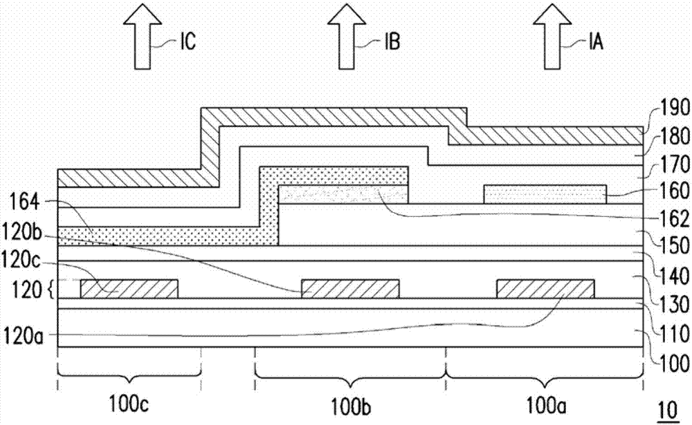
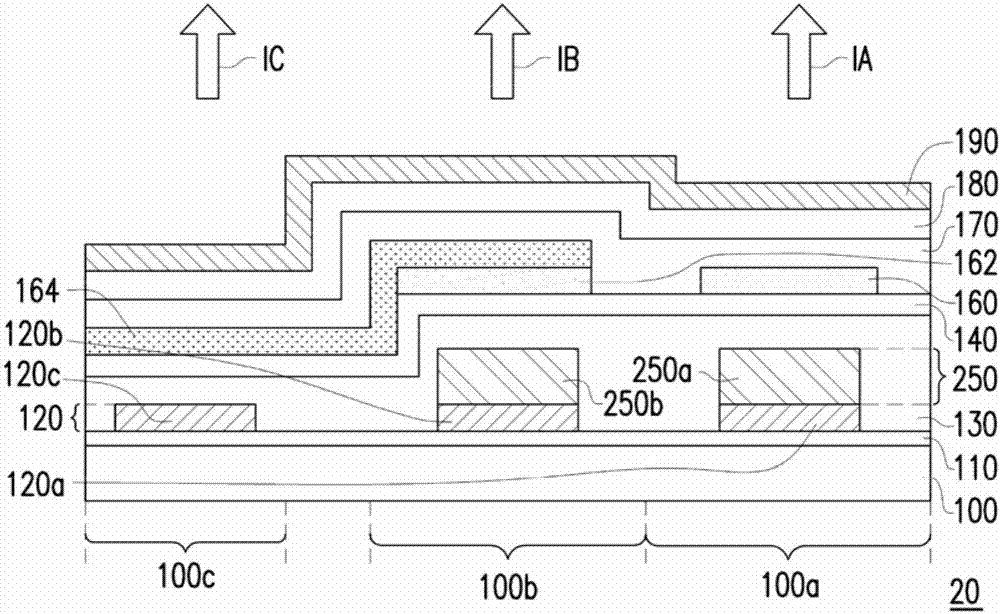
[0040] The pixel structure of the present invention can be applied in OLED display panels, for example. Based on this, although in order to describe the design of the pixel structure of the present invention in detail, the following is an example of a single pixel structure, but any person skilled in the art should understand that an organic light emitting diode display panel generally includes multiple identical or A pixel array formed by arrays of similar pixel structures. Therefore, anyone skilled in the art can understand the structure or layout of the pixel array in the OLED display panel according to the following description for a single pixel structure.

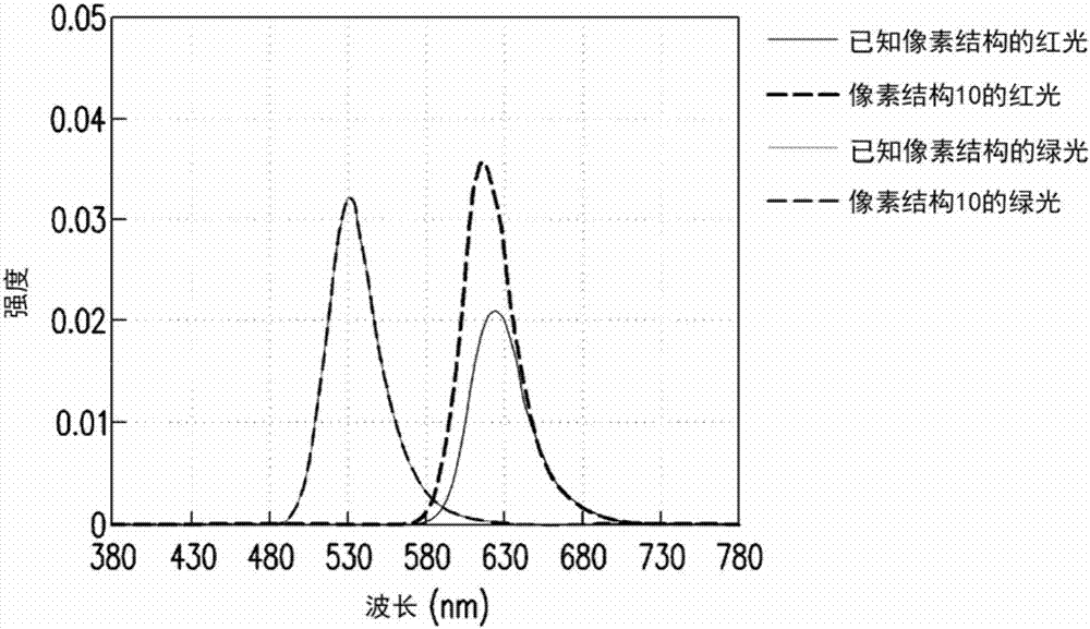
[0041] figure 1 is a schematic cross-sectional view of the pixel structure according to the first embodiment of the present invention. Please refer to figure 1 , ...


PUM


Abstract

A pixel structure includes a substrate, a first electrode layer, a second electrode layer, a first light-emitting layer, a second light-emitting layer, a third light-emitting layer, and a thickened layer. The substrate includes first, second, and third sub-pixel regions. The first and second electrode layers are disposed on the substrate and located in the first, second and third sub-pixel regions. The first, second and third light-emitting layers are disposed between the first electrode layer and the second electrode layer, the first light-emitting layer is located in the first sub-pixel area, the second light-emitting layer is located in the second sub-pixel area, the third The light-emitting layer is located in the second and third sub-pixel regions, and the third light-emitting layer and the second light-emitting layer overlap in the second sub-pixel region. The first and second light-emitting layers are disposed on a side of the thickening layer opposite to the first electrode layer, and the thickening layer is a single structure layer and located only in the first and second sub-pixel regions.

Description

technical field [0001] The present invention relates to a pixel structure, and in particular to a pixel structure for an organic electroluminescence display panel. Background technique [0002] Organic electroluminescent display panels (such as organic light-emitting diodes (OLEDs) display panels) have the advantages of active light emission, high contrast, thin thickness and wide viewing angle, and are expected to become the mainstream products of the new generation of flat display panels. [0003] Due to the resonant cavity effect of the OLED display panel, its high efficiency and high color purity can be exhibited through proper optical design. In the side-by-side (SBS) OLED display panel of the prior art, the light-emitting layer generally needs to be evaporated separately for the RGB sub-pixels using a fine metal mask (FMM). In order to meet the resonant cavity effect, besides the light-emitting layer, other layers still need to use FMM to adjust the light color and in...

Claims


Application Information

Patent Timeline
Patent Type & Authority Applications(China)
IPC IPC(8): H01L27/32H01L51/50
CPCH10K59/353H10K50/11H10K50/15
Inventor 吴忻蕙林冠亨陈重嘉李孟庭
Owner AU OPTRONICS CORP
Features
  • R&D
  • Intellectual Property
  • Life Sciences
  • Materials
  • Tech Scout
  • Unparalleled Data Quality
  • Higher Quality Content
  • 60% Fewer Hallucinations
Learn More