Supercharge Your Innovation With Domain-Expert AI Agents!

Capacitively coupled plasma processing device and plasma processing method

A plasma and processing device technology, applied in the field of plasma processing devices

Active Publication Date: 2020-02-11
ADVANCED MICRO FAB EQUIP INC CHINA
View PDF16 Cites 0 Cited by
  • Summary
  • Abstract
  • Description
  • Claims
  • Application Information

AI Technical Summary

Problems solved by technology

[0006] However, existing capacitively coupled plasma processing devices still have room for improvement, especially in terms of processing uniformity

Method used


Image

  • Capacitively coupled plasma processing device and plasma processing method
  • Capacitively coupled plasma processing device and plasma processing method
  • Capacitively coupled plasma processing device and plasma processing method

Examples


Embodiment Construction

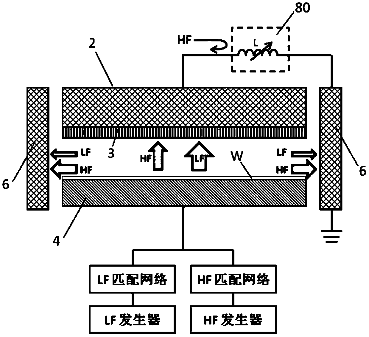
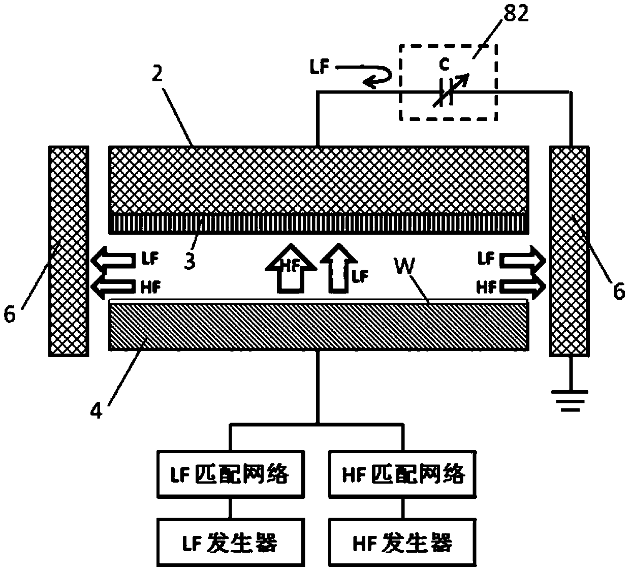
[0040] The capacitively coupled plasma processing apparatus and method of the present invention will be described below with reference to specific embodiments and accompanying drawings. It should be emphasized that the illustration here is only an example, and other implementations utilizing the present invention are not excluded.

[0041] The capacitively coupled plasma processing apparatus according to the present invention includes a reaction chamber enclosed by a plurality of walls (such as side walls, top walls and bottom walls), and a space is provided inside the reaction chamber. The reaction chamber can be evacuated. Except for the air inlet, the exhaust port and the passage for the substrate to enter and exit, other parts of the reaction chamber are kept airtight and isolated from the outside world during the processing. The gas inlet is connected with an external gas source, and is used for continuously supplying processing gas to the reaction chamber during the pro...


PUM


Abstract

The invention provides a capacitively-coupled plasma processing apparatus and a plasma processing method, and aims to improve semiconductor processing uniformity. The capacitively-coupled plasma processing apparatus comprises a reaction cavity, an upper electrode, a lower electrode, a radio frequency power source, a bias power source and an impedance regulation apparatus, wherein the reaction cavity has a top wall, side walls and a bottom wall; the upper electrode is arranged on the top wall; the lower electrode is positioned in the reaction cavity, and arranged opposite to the upper electrode; the radio frequency power source is applied to the lower electrode; the bias power source is applied to the lower electrode; and one end of the impedance regulation apparatus is connected to the upper electrode or the side walls while the other end is grounded.

Description

technical field [0001] The present invention relates to a capacitively coupled plasma (Capacitively Coupled Plasma) processing device for processing semiconductor devices, such as a capacitively coupled plasma etching device, a capacitively coupled plasma deposition device, etc., and also relates to a method for processing semiconductor devices using the above device. Background technique [0002] In the manufacturing process of semiconductor devices, in order to form a predetermined pattern on a predetermined layer formed on a semiconductor wafer as a substrate to be processed, a plasma etching process using a resist as a mask and etching with plasma is often used . [0003] As a plasma etching apparatus for performing such plasma etching, various apparatuses are used, and capacitively coupled plasma processing apparatuses are mainly used. [0004] In the capacitively coupled plasma etching device, a pair of parallel plate electrodes (upper and lower electrodes) are arrang...

Claims


Application Information

Patent Timeline
Patent Type & Authority Patents(China)
IPC IPC(8): H01J37/32
CPCH01J37/32091H01J37/32183
Inventor 叶如彬梁洁涂乐义徐朝阳杨金全
Owner ADVANCED MICRO FAB EQUIP INC CHINA
Features
  • R&D
  • Intellectual Property
  • Life Sciences
  • Materials
  • Tech Scout
  • Unparalleled Data Quality
  • Higher Quality Content
  • 60% Fewer Hallucinations
Learn More