Peak power probe hardware adjustment zero offset circuit and method

A peak power and zero adjustment technology, applied in the field of zero offset adjustment of peak power probe hardware, can solve the problems of high channel noise, complex circuit, poor sensitivity, etc., and achieve the effect of low channel noise, high sensitivity index, and simple circuit

Inactive Publication Date: 2017-11-03
THE 41ST INST OF CHINA ELECTRONICS TECH GRP
View PDF5 Cites 3 Cited by
  • Summary
  • Abstract
  • Description
  • Claims
  • Application Information

AI Technical Summary

Problems solved by technology

[0006] (1) Using a single-ended operational amplifier, the channel noise is high and the sensitivity is poor;
[0007] (2) Due to the low performance index of the high-speed ADC device at that time, it was necessary to use a high-digit low-speed ADC and a high-gain amplifier circuit to adjust the zero point offset, and the circuit was more complicated;

Method used


Image

  • Peak power probe hardware adjustment zero offset circuit and method
  • Peak power probe hardware adjustment zero offset circuit and method
  • Peak power probe hardware adjustment zero offset circuit and method

Examples


Embodiment Construction

[0046] The following will clearly and completely describe the technical solutions in the embodiments of the present invention with reference to the accompanying drawings in the embodiments of the present invention. Obviously, the described embodiments are only some, not all, embodiments of the present invention. Based on the embodiments of the present invention, all other embodiments obtained by persons of ordinary skill in the art without making creative efforts belong to the protection scope of the present invention.

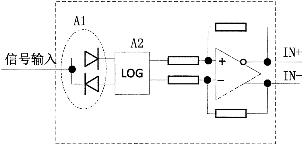
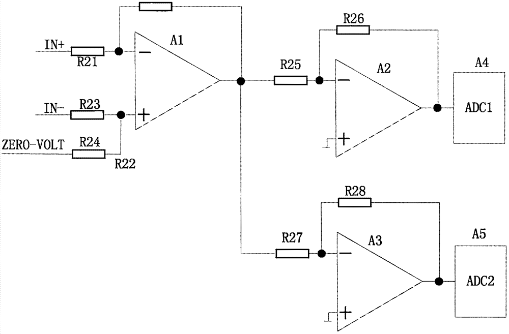
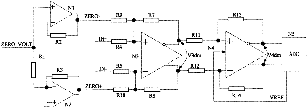
[0047] Such as image 3 As shown, the present invention proposes a peak power probe hardware adjustment zero point offset circuit and method. The idea of ​​hardware adjustment zero point offset is: when the peak power probe has no signal input, due to temperature changes or peak power probes are connected to different After IN+ and IN- change due to the test equipment, set the DAC value and change the ZERO_VOLT voltage value to keep the voltage value of the A / ...


PUM


Abstract

The present invention provides a peak power probe hardware adjustment zero offset circuit. The circuit comprises two stages of differential amplifiers; the first-stage differential amplifier and peripheral resistors are matched with each other so as to constitute a differential adder; the forward input end of the first-stage differential amplifier is connected with a zero offset adjustment voltage and + signals inputted by a peak power probe; the reverse input end of the first-stage differential amplifier is connected with the reverse signal of the zero offset adjustment voltage and - signals inputted by the peak power probe; the second-stage differential amplifier and peripheral resistors are matched with each other so as to constitute a differential driving amplifier of an ADC; the gain of front-stage input signals is adjusted, and at the same time, the common-mode voltage of the input signals is increased, wherein the common-mode voltage is provided by the reference voltage of the ADC; and the zero offset adjustment voltage is set through a DAC, so that a difference-mode voltage outputted by the second-stage differential amplifier is a constant value when no signals are inputted into the peak power probe. The peak power probe hardware adjustment zero offset circuit of the invention has the advantages of higher zero adjustment voltage accuracy index, higher power accuracy index, low channel noises, high sensitivity index and simplicity.

Description

technical field [0001] The invention relates to the technical field of testing, in particular to a peak power probe hardware adjustment zero point offset circuit, and also relates to a peak power probe hardware adjustment zero point offset method. Background technique [0002] In peak power measurement, adjusting the zero offset is an important means to ensure the accuracy and sensitivity of power measurement. [0003] figure 1 A schematic diagram of a peak power sensor is shown, A1 is a detector consisting of a diode pair, and A2 is a logarithmic amplifier. In the case of no signal input, if the ambient temperature changes greatly, or the peak power probe is connected to different test equipment, the output IN+ and IN- of the probe will have a relatively large change due to the change of the noise floor, thus This results in relatively large changes in the ADC value sampled at the back end, and a relatively large change in the measured noise floor power, which affects the...

Claims


Application Information

Patent Timeline
Patent Type & Authority Applications(China)
IPC IPC(8): G01R35/00G01R21/00H03F3/68
CPCG01R35/005G01R21/00H03F3/68
Inventor 李金山李强刘元商冷朋徐达旺赵浩
Owner THE 41ST INST OF CHINA ELECTRONICS TECH GRP
Why Eureka
Try Eureka