Array substrate
An array substrate and substrate technology, applied in nonlinear optics, instruments, optics, etc., can solve the problems affecting the signal transmission stability of deep holes and shallow holes, increase the height, and the risk of high vertical alignment abnormality, so as to compensate for the decrease in charge transmission rate , stable signal transmission, reducing the effect of abnormal alignment
- Summary
- Abstract
- Description
- Claims
- Application Information
AI Technical Summary
Problems solved by technology
Method used
Image

Examples
Embodiment Construction
[0035] The present invention will be further described below in conjunction with accompanying drawing.
[0036] Such as figure 1 , showing an array substrate comprising:
[0037] Substrate (not shown in the figure);
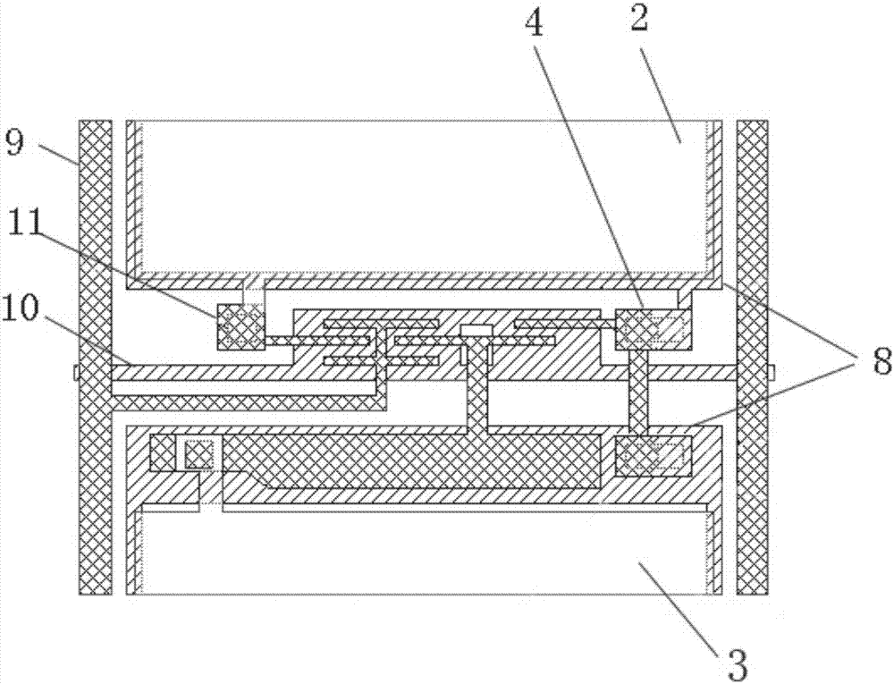
[0038] A plurality of pixel units 1 located on the substrate, each pixel unit 1 includes a main pixel electrode 2, a sub-pixel electrode 3, and a deep and shallow hole unit 4 for pulling down the potential of the sub-pixel electrode 3;
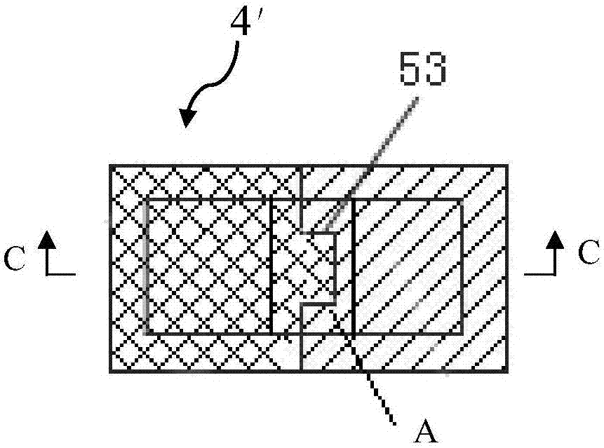
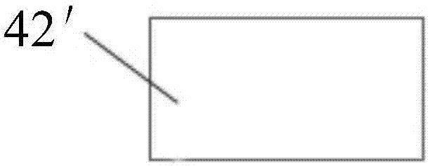
[0039] Such as Figure 7 As shown, the deep and shallow hole unit 4 includes a film stack layer 41 having deep holes and shallow holes and a floating conductive layer 42 located on the film stack layer 41 . Such as Figure 5 and Figure 6 As shown, the floating conductive layer 42 corresponds to the junction of the deep hole and the shallow hole (such as Figure 5 The position shown in A) has an opening 421, and the floating conductive layer 42 has protrusions 422 on both sides corresponding to the junction of the deep hol...
PUM
 Abstract
Description
Claims
Application Information
 - R&D
- Intellectual Property
- Life Sciences
- Materials
- Tech Scout
- Unparalleled Data Quality
- Higher Quality Content
- 60% Fewer Hallucinations
Browse by: Latest US Patents, China's latest patents, Technical Efficacy Thesaurus, Application Domain, Technology Topic, Popular Technical Reports.
© 2025 PatSnap. All rights reserved.Legal|Privacy policy|Modern Slavery Act Transparency Statement|Sitemap|About US| Contact US: help@patsnap.com