Filling-sealing method of circuit structure and filling-sealing circuit structure

A technology of circuit structure and potting, which is applied in the direction of circuits, transformer/inductance parts, electrical components, etc., and can solve problems such as inductive drop

Pending Publication Date: 2017-11-07
SHENZHEN SOSEN ELECTRONICS CO LTD
View PDF6 Cites 3 Cited by
  • Summary
  • Abstract
  • Description
  • Claims
  • Application Information

AI Technical Summary

Problems solved by technology

[0007] The technical problem to be solved by the present invention is to provide a potting method of a circuit structure for the defects in the prior art that the joint of the magnetic core of the inductance device is easily squeezed by the potting glue, which causes the inductance to drop after potting. Potting circuit structure

Method used


Image

  • Filling-sealing method of circuit structure and filling-sealing circuit structure
  • Filling-sealing method of circuit structure and filling-sealing circuit structure
  • Filling-sealing method of circuit structure and filling-sealing circuit structure

Examples


Embodiment Construction

[0030] In order to make the object, technical solution and advantages of the present invention clearer, the present invention will be further described in detail below in conjunction with the accompanying drawings and embodiments. It should be understood that the specific embodiments described here are only used to explain the present invention, not to limit the present invention.

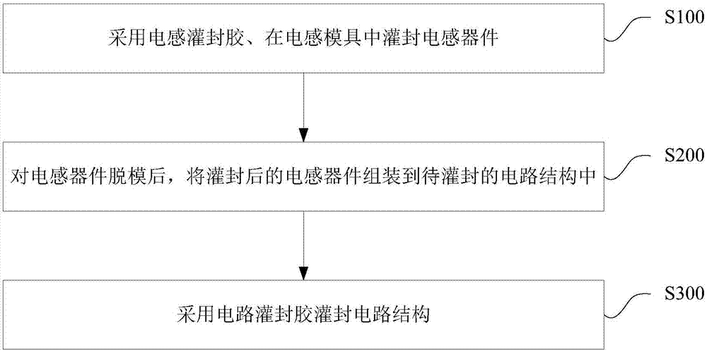
[0031] figure 1 A flowchart showing a potting method for a circuit structure according to an embodiment of the present invention, the circuit structure includes a plurality of components, and at least one inductance device is included in the plurality of components. The potting method includes: step S100, using inductance potting glue, potting the inductance device in the inductance mold; step S200, after demoulding the inductance device, assembling the potted inductance device into the circuit structure to be potted ; and step S300 , encapsulating the circuit structure with a circuit encapsulant....


PUM

PropertyMeasurementUnit
thermal resistanceaaaaaaaaaa
hardnessaaaaaaaaaa
hardnessaaaaaaaaaa

Abstract

The invention relates to a filling-sealing method of a circuit structure and a filling-sealing circuit structure. The filling-sealing method comprises the steps that an inductance mold is fill-sealed with an inductance pouring sealant to form an inductance device; after the inductance device is demolded, the fill-sealed inductance device is assembled in the circuit structure to be fill-sealed; the circuit structure is fill-sealed by adopting a circuit pouring sealant. The filling-sealing circuit structure comprises multiple components, at least one inductance device in the multiple components is coated or covered by fill-sealing inductance pouring sealant, and the inductance devices coated or covered with the inductance pouring sealant and other components are coated or covered by fill-sealing the circuit pouring sealant. Before the inductance devices and other components are fill-sealed together, the components are already coated with the inductance pouring sealant through primary fill-sealing, the coated inductance pouring sealant can protect a magnetic core of each inductance device against stress impact of the circuit pouring sealant in whole circuit structure fill-sealing, accordingly inductance quantity decrease is prevented, and EMC performance is ensured.

Description

technical field [0001] The invention relates to the field of circuits and circuit potting, in particular to a potting method for a circuit structure and a potting circuit structure. Background technique [0002] Many circuit structures contain inductive devices, such as common-mode inductors in power supplies (also called common-mode choke coils), which are often used to suppress common-mode electromagnetic interference signals in power supplies so that the power supplies comply with relevant electromagnetic interference standards. The magnetic circuit form of common mode inductors has open magnetic circuit (composed of two parts, such as PK type, UU type, EE type, etc.), and also has closed magnetic circuit type (such as T ring, SQ type, ET type, etc.). Conductivity is typically 5000 to 15000. [0003] Taking the open magnetic common mode inductor as an example, it has been widely used because of its advantages in cost, volume, and reliability, especially in the applicatio...

Claims


Application Information

Patent Timeline
Patent Type & Authority Applications(China)
IPC IPC(8): H01F41/00H01F27/02
CPCH01F27/022H01F41/005
Inventor 王宗友邹超洋杨千
Owner SHENZHEN SOSEN ELECTRONICS CO LTD
Why Eureka
Try Eureka