
OLED double-sided displayer and manufacturing method thereof

A technology of double-sided display and manufacturing method, which is applied in semiconductor/solid-state device manufacturing, electric solid-state devices, semiconductor devices, etc., can solve the problems of thick structure, high manufacturing cost, complicated process, etc. The effect of simple method

Inactive Publication Date: 2017-11-07
WUHAN CHINA STAR OPTOELECTRONICS SEMICON DISPLAY TECH CO LTD
View PDF12 Cites 12 Cited by
  • Summary
  • Abstract
  • Description
  • Claims
  • Application Information

AI Technical Summary

Problems solved by technology

However, in this design, there is an obvious disadvantage, that is, the image displayed on the front of the panel and the image displayed on the back of the panel are in a mirror image relationship, that is, the images seen by the observer on the left and right sides of the pattern are reversed, which gives the observer It brings a lot of inconvenience, especially when the panel displays a map-type image, this disadvantage is particularly significant
[0005] Another commonly used OLED double-sided display design is to attach two top-emitting OLED panels back to back, and respectively inject signals through two integrated circuits (ICs), so that the images displayed on the front and back sides There will be no problem of directional distortion when observing, but this design has an obvious disadvantage, that is, it needs two independent OLED panels, the structure is relatively thick, the process is relatively complicated, the production cost is high, and it does not meet consumer expectations. and cost-effective requirements

Method used


Image

  • OLED double-sided displayer and manufacturing method thereof
  • OLED double-sided displayer and manufacturing method thereof
  • OLED double-sided displayer and manufacturing method thereof

Examples


Embodiment Construction

[0036] In order to further illustrate the technical means adopted by the present invention and its effects, the following describes in detail in conjunction with preferred embodiments of the present invention and accompanying drawings.

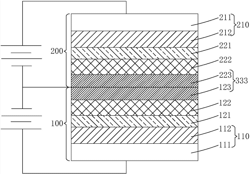
[0037] see figure 1 , the present invention firstly provides an OLED double-sided display, including a first OLED light-emitting substrate 100 and a second OLED light-emitting substrate 200 disposed opposite to each other;

[0038] Wherein, the first OLED light-emitting substrate 100 includes a first substrate 110 and a first pixel electrode layer 121 and a first OLED organic functional layer 122 arranged in sequence on the side of the first substrate 110 close to the second OLED light-emitting substrate 200 and the first reflective cathode layer 123; thus the first pixel electrode layer 121, the first OLED organic functional layer 122 and the first reflective cathode layer 123 together constitute the first OLED light-emitting layer 120, and t...


PUM


Abstract

The invention provides an OLED double-sided displayer and a manufacturing method thereof. The OLED double-sided displayer comprises a first OLED light-emitting substrate and a second OLED light-emitting substrate which are oppositely arranged. The respective first reflecting cathode layer and the second reflecting cathode layer of the first OLED light-emitting substrate and the second OLED light-emitting substrate are adhered together through conductive ink so as to form a total cathode layer together, and then the first OLED light-emitting substrate and the second OLED light-emitting substrate are adhered together through the conductive ink in a facing way. The manufacturing method is simple, the cost is low, the problems of thickness and weight of the present double-sided displayer can be effectively solved, and the front and rear surfaces of the OLED double-sided displayer are enabled to display different frames simultaneously.

Description

technical field [0001] The invention relates to the field of display technology, in particular to an OLED double-sided display and a manufacturing method thereof. Background technique [0002] Organic light emitting diode (OLED) display has self-illumination, low driving voltage, high luminous efficiency, short response time, high definition and contrast, wide viewing angle, wide operating temperature range, and can realize flexible display and large-area full-screen With many advantages such as color display, it is recognized by the industry as the display device with the most development potential. The OLED display is a self-luminous display device, and the OLED light-emitting device on it usually includes a pixel electrode and a common electrode used as an anode (Anode) and a cathode (cathode) respectively, and an organic functional layer arranged between the pixel electrode and the common electrode. These organic functional layers emit light when an electric current is ...

Claims


Application Information

Patent Timeline
Patent Type & Authority Applications(China)
IPC IPC(8): H01L27/32H01L51/52H01L51/56
CPCH10K59/128H10K50/82H10K71/00
Inventor 徐超
Owner WUHAN CHINA STAR OPTOELECTRONICS SEMICON DISPLAY TECH CO LTD
Learn More